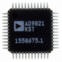
AD9821KSTZ Analog Devices Inc, AD9821KSTZ Datasheet

AD9821KSTZ
Specifications of AD9821KSTZ
Available stocks
Related parts for AD9821KSTZ
AD9821KSTZ Summary of contents
Page 1
FEATURES Differential Sensor Input with 1 V p-p Input Range 10-Bit Variable Gain Amplifier (VGA) Low Noise Optical Black Clamp Circuit Analog Preblanking Function 12-Bit 40 MSPS A/D Converter (ADC) 3-Wire Serial Digital Interface 3 ...
Page 2
AD9821–SPECIFICATIONS GENERAL SPECIFICATIONS Parameter TEMPERATURE RANGE Operating Storage POWER SUPPLY VOLTAGE Analog, Digital, Digital Driver POWER CONSUMPTION Normal Operation Power-Down Modes Standby Total Power-Down MAXIMUM CLOCK RATE A/D CONVERTER Resolution Differential Nonlinearity (DNL) No Missing Codes Full-Scale Input Voltage Data ...
Page 3
IMAGER-MODE SPECIFICATIONS Parameter P OWER CONSUMPTION MAXIMUM CLOCK RATE ANALOG INPUTS (VIN+, VIN–) Input Common-Mode Range* Max Input Amplitude* Max Optical Black Pixel Amplitude* VARIABLE GAIN AMPLIFIER (VGA) Gain Control Resolution Gain Monotonicity Gain Range Min Gain (VGA Gain Code ...
Page 4
AD9821 TIMING SPECIFICATIONS Parameter SAMPLE CLOCKS DATACLK Clock Period DATACLK Hi/Low Pulsewidth CLPOB Pulsewidth* Internal Clock Delay DATA OUTPUTS Output Delay Output Hold Time Pipeline Delay SERIAL INTERFACE Maximum SCK Frequency SL to SCK Setup Time SCK to SL Hold ...
Page 5
CONNECT Pin Number Mnemonic 1–12 D0–D11 13 DRVDD 14 DRVSS 15, 41 DVSS 16 DATACLK 17 DVDD1 18, 24, 37, 42, 47 PBLK 20 CLPOB 21–23 TEST 25, 26, 35 AVSS 27 AVDD1 28, ...
Page 6
AD9821 DEFINITIONS OF SPECIFICATIONS Differential Nonlinearity (DNL) An ideal ADC exhibits code transitions that are exactly 1 LSB apart. DNL is the deviation from this ideal value. Thus, every code must have a finite width. No missing codes guaranteed to ...
Page 7
V DD 130 120 110 100 20 30 SAMPLE RATE – MHz TPC 1. Power vs. Sample Rate 1.0 0.5 0 –0.5 –1.0 0 500 1000 1500 2000 2500 TPC 2. Typical DNL Performance REV. 0 Typical ...
Page 8
AD9821 IMAGER MODE AND AUX MODE TIMING N VIN VIN– DATACLK t OD OUTPUT N–10 DATA NOTES: 1. VIN+ AND VIN– SIGNALS ARE SAMPLED AT DATACLK RISING EDGES (CAN BE INVERTED USING THE CONTROL REGISTER). 2. INTERNAL SAMPLING ...
Page 9
INTERNAL REGISTER MAP AND SERIAL INTERFACE TIMING Register Address Name Operation Input Mode Selection VGA Gain LSB Clamp Level LSB 1 Control ...
Page 10
AD9821 REGISTER DETAILS Table II. Operation Register Contents (Default Value x000) Optical Black Clamp D10 Enable Clamping 1 Disable Clamping NOTES 1 Must be ...
Page 11
CIRCUIT DESCRIPTION AND OPERATION The AD9821 signal processing chain is shown in Figure 10. Each processing step is essential in achieving a high quality image from the raw imager pixel data. Differential Input SHA The differential input SHA circuit is ...
Page 12
AD9821 Variable Gain Amplifier The VGA stage provides a gain range dB, program- mable with 10-bit resolution through the serial digital interface. A minimum gain needed to match ...
Page 13
APPLICATIONS INFORMATION The AD9821 is a complete Analog Front End (AFE) product for a variety of imager applications using CMOS image sensors and CCDs with on-chip CDS. As shown in Figure 10, the imager output is generally buffered and sent ...
Page 14
AD9821 Internal Power-On Reset Circuitry After power-on, the AD9821 will automatically reset all internal registers and perform internal calibration procedures. This takes approximately complete. During this time, normal clock signals and serial write operations may occur. However, ...
Page 15
SEATING 0.05 PLANE ROTATED 90 CCW REV. 0 OUTLINE DIMENSIONS 48-Lead Plastic Quad Flatpack [LQFP] 1.4 mm Thick (ST-48) Dimensions shown in millimeters 1.60 MAX PIN 1 INDICATOR 0.75 0.60 0.45 SEATING PLANE 0.20 0.09 VIEW ...
Page 16
–16– ...


