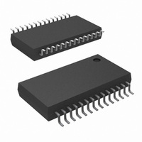
DS92LV1212AMSA/NOPB National Semiconductor, DS92LV1212AMSA/NOPB Datasheet

DS92LV1212AMSA/NOPB
Specifications of DS92LV1212AMSA/NOPB
*DS92LV1212AMSA/NOPB
DS92LV1212AMSA
Available stocks
Related parts for DS92LV1212AMSA/NOPB
DS92LV1212AMSA/NOPB Summary of contents
Page 1
... SYNC patterns. Block Diagram TRI-STATE ® registered trademark of National Semiconductor Corporation. © 2000 National Semiconductor Corporation Features n Clock recovery without SYNC patterns-random lock n Guaranteed transition every data transfer cycle ...
Page 2
Block Diagram (Continued) Functional Description The DS92LV1212 is a 10-bit Deserializer chip designed to receive data over heavily loaded differential backplanes at clock speeds from 16 MHz to 40 MHz. It may also be used to receive data over Unshielded ...
Page 3
Resynchronization (Continued) recommendation is to provide a feedback loop using the LOCK pin itself to control the sync request of the Serializer (SYNC1 or SYNC2). Dual SYNC pins are provided for mul- tiple control in a multi-drop application. Sending sync ...
Page 4
RMT Patterns DIN0 Held Low-DIN1 Held High Creates an RMT Pattern DIN8 Held Low-DIN9 Held High Creates an RMT Pattern NSID DS92LV1021TMSA DS92LV1212AMSA www.national.com DS101387-23 DIN4 Held Low-DIN5 Held High Creates an RMT Pattern DS101387-25 Order Numbers Function Serializer Deserializer ...
Page 5
... Absolute Maximum Ratings If Military/Aerospace specified devices are required, please contact the National Semiconductor Sales Office/ Distributors for availability and specifications. Supply Voltage ( CMOS/TTL Input Voltage CMOS/TTL Output Voltage Bus LVDS Receiver Input Voltage Junction Temperature Storage Temperature Lead Temperature (Soldering, 4 seconds) ...
Page 6
Deserializer Switching Characteristics Over recommended operating supply and temperature ranges unless otherwise specified. Symbol Parameter t Receiver out Clock RCP Period t CMOS/TTL Low-to-High CLH Transition Time t CMOS/TTL High-to-Low CHL Transition Time t Deserializer Delay DD t ROUT (0-9) ...
Page 7
AC Timing Diagrams and Test Circuits FIGURE 1. “Worst Case” Deserializer ICC Test Pattern FIGURE 2. Deserializer CMOS/TTL Output Load and Transition Times FIGURE 3. Serializer Delay FIGURE 4. Deserializer Delay 7 DS101387-4 DS101387-6 DS101387-11 DS101387-12 www.national.com ...
Page 8
AC Timing Diagrams and Test Circuits Timing shown for RCLK_R/F = LOW Duty Cycle ( RDC FIGURE 6. Deserializer TRI-STATE Test Circuit and Timing www.national.com (Continued) FIGURE 5. Deserializer Setup and Hold Times 8 DS101387-13 DS101387-14 ...
Page 9
AC Timing Diagrams and Test Circuits FIGURE 7. Deserializer PLL Lock Times and PWRDN TRI-STATE Delays FIGURE 8. Deserializer PLL Lock Time from SyncPAT (Continued) 9 DS101387-15 DS101387-22 www.national.com ...
Page 10
AC Timing Diagrams and Test Circuits SW - Setup and Hold Time (Internal data sampling window Serializer Output Bit Position Jitter JIT t = Receiver Sampling Margin Time RSM Application Information Using the DS92LV1021 and DS92LV1212A The Serializer ...
Page 11
Application Information the receiver end. Please note that in point-to-point configu- ration, the potential of offsetting the ground levels of the Serializer vs. the Deserializer must be considered. Also, Bus LVDS provides a +/− 1.2V common mode range at the ...
Page 12
Application Information Note: For the DS92LV1021, t FIGURE 12. Using t DJIT www.national.com (Continued) (max) = 70pS and t DJIT and t to Generate an Eye Pattern Mask and Validate SIgnal Quality RNM 12 DS101387-28 (min) = −300pS DJIT ...
Page 13
Pin Diagram Deserializer Pin Description Pin Name I/O ROUT O RCLK_R/F I RI+ I RI− I PWRDN I LOCK O RCLK O REN I DVCC I DGND I AVCC I AGND I REFCLK I DS92LV1212AMSA - Deserializer DS101387-19 No. ± ...
Page 14
Truth Table INPUTS PWRDN REN LOCK Active indicates the LOCK output will reflect the state of the Deserializer with regard to the selected data stream. 2) RCLK Active indicates the RCLK will ...
Page 15
... NATIONAL’S PRODUCTS ARE NOT AUTHORIZED FOR USE AS CRITICAL COMPONENTS IN LIFE SUPPORT DEVICES OR SYSTEMS WITHOUT THE EXPRESS WRITTEN APPROVAL OF THE PRESIDENT AND GENERAL COUNSEL OF NATIONAL SEMICONDUCTOR CORPORATION. As used herein: 1. Life support devices or systems are devices or systems which, (a) are intended for surgical implant ...


