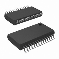
DS92LV1021AMSA/NOPB National Semiconductor, DS92LV1021AMSA/NOPB Datasheet

DS92LV1021AMSA/NOPB
Specifications of DS92LV1021AMSA/NOPB
*DS92LV1021AMSA/NOPB
DS92LV1021AMSA
Available stocks
Related parts for DS92LV1021AMSA/NOPB
DS92LV1021AMSA/NOPB Summary of contents
Page 1
... In addition, the embedded clock guarantees a Block Diagrams TRI-STATE ® registered trademark of National Semiconductor Corporation. © 2003 National Semiconductor Corporation transition on the bus every 12-bit cycle. This eliminates transmission errors due to charged cable conditions. Fur- thermore, you may put the DS92LV1021A output pins into TRI-STATE ® ...
Page 2
Block Diagrams (Continued) Functional Description The DS92LV1021A is an upgrade to the DS92LV1021. The DS92LV1021A no longer has a power-up sequence require- ment. Like the DS92LV1021, the DS92LV1021A is a 10-bit Serializer designed to transmit data over a differential back- ...
Page 3
Resynchronization (Continued) LOCK pin itself to control the sync request of the Serializer (SYNC1 or SYNC2). At the time of publication, other than the DS92LV1210, all other Deserializers from National Semicon- ductor have random lock capability. This feature does not ...
Page 4
... Absolute Maximum Ratings If Military/Aerospace specified devices are required, please contact the National Semiconductor Sales Office/ Distributors for availability and specifications. Supply Voltage ( CMOS/TTL Input Voltage −0. CMOS/TTL Output Voltage −0. Bus LVDS Receiver Input Voltage Bus LVDS Driver Output Voltage Bus LVDS Output Short ...
Page 5
Serializer Timing Requirements for TCLK Over recommended operating supply and temperature ranges unless otherwise specified. Symbol Parameter t Transmit Clock Period TCP t Transmit Clock High Time TCIH t Transmit Clock Low Time TCIL t TCLK Input Transition CLKT Time ...
Page 6
AC Timing Diagrams and Test Circuits FIGURE 1. “Worst Case” Serializer ICC Test Pattern FIGURE 2. Serializer Bus LVDS Output Load and Transition Times Timing shown for TCLK_R/F = LOW www.national.com FIGURE 3. Serializer Input Clock Transition Time FIGURE 4. ...
Page 7
AC Timing Diagrams and Test Circuits FIGURE 5. Serializer TRI-STATE Test Circuit and Timing FIGURE 6. Serializer PLL Lock Time, and PWRDN TRI-STATE Delays (Continued) 20026909 7 20026925 www.national.com ...
Page 8
AC Timing Diagrams and Test Circuits www.national.com (Continued) FIGURE 7. SYNC Timing Delays FIGURE 8. Serializer Delay 8 20026926 20026911 ...
Page 9
AC Timing Diagrams and Test Circuits For an explanation of the Ideal Crossing Point, please see the Application Information Section. FIGURE 9. Serializer Deterministic Jitter and Ideal Crossing Point Application Information DIFFERENCES BETWEEN THE DS92LV1021A AND THE DS92LV1021 The DS92LV1021A ...
Page 10
Application Information PCB CONSIDERATIONS The Bus LVDS devices Serializer and Deserializer should be placed as close to the edge connector as possible. In mul- tiple Deserializer applications, the distance from the Deseri- alizer to the slot connector appears as a ...
Page 11
Serializer Pin Description Pin Name I/O DIN I TCLK_R/F I DO+ O DO− O DEN I PWRDN I TCLK I SYNC I DVCC I DGND I AVCC I AGND I Truth Table DIN (0–9) TCLK_R/F TCLK ...
Page 12
... NATIONAL’S PRODUCTS ARE NOT AUTHORIZED FOR USE AS CRITICAL COMPONENTS IN LIFE SUPPORT DEVICES OR SYSTEMS WITHOUT THE EXPRESS WRITTEN APPROVAL OF THE PRESIDENT AND GENERAL COUNSEL OF NATIONAL SEMICONDUCTOR CORPORATION. As used herein: 1. Life support devices or systems are devices or systems which, (a) are intended for surgical implant ...


