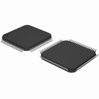
DS92LV18TVV/NOPB National Semiconductor, DS92LV18TVV/NOPB Datasheet

DS92LV18TVV/NOPB
Specifications of DS92LV18TVV/NOPB
*DS92LV18TVV/NOPB
DS92LV18TVV
Available stocks
Related parts for DS92LV18TVV/NOPB
DS92LV18TVV/NOPB Summary of contents
Page 1
... EMI by coupling the result- ing fringing fields together. Block Diagram TRI-STATE ® registered trademark of National Semiconductor Corporation. © 2006 National Semiconductor Corporation Features n 15–66 MHz 18:1/1:18 Serializer/Deserializer (2.376 Gbps full duplex throughput) n Independent transmitter and receiver operation with ...
Page 2
... Absolute Maximum Ratings If Military/Aerospace specified devices are required, please contact the National Semiconductor Sales Office/ Distributors for availability and specifications. Supply Voltage ( LVCMOS/LVTTL Input Voltage −0. LVCMOS/LVTTL Output Voltage −0. Bus LVDS Receiver Input Voltage Bus LVDS Driver Output Voltage Bus LVDS Output Short ...
Page 3
Electrical Characteristics Over recommended operating supply and temperature ranges unless otherwise specified. Symbol Parameter Output Differential Voltage V OD (DO+) - (DO-) Output Differential Voltage ∆V OD Unbalance V Offset Voltage OS ∆V Offset Voltage Unbalance OS I Output Short ...
Page 4
Serializer Switching Characteristics Over recommended operating supply and temperature ranges unless otherwise specified. Symbol Parameter ± DO HIGH to t HZD TRI-STATE Delay ± DO LOW to t LZD TRI-STATE Delay ± DO TRI-STATE to t ZHD HIGH Delay ± ...
Page 5
Deserializer Switching Characteristics Over recommended operating supply and temperature ranges unless otherwise specified. Symbol Parameter Conditions HIGH to TRI-STATE t HZR Delay LOW to TRI-STATE t LZR Delay Figure 13 TRI-STATE to HIGH t ZHR Delay TRI-STATE to LOW t ...
Page 6
AC Timing Diagrams and Test Circuits FIGURE 1. “Worst Case” Serializer ICC Test Pattern FIGURE 2. “Worst Case” Deserializer ICC Test Pattern FIGURE 3. Serializer Bus LVDS Distributed Output Load and Transition Times FIGURE 4. Deserializer CMOS/TTL Distributed Output Load ...
Page 7
AC Timing Diagrams and Test Circuits FIGURE 5. Serializer Input Clock Transition Time FIGURE 7. Serializer TRI-STATE Test Circuit and Timing (Continued) FIGURE 6. Serializer Setup/Hold Times 7 20031207 20031208 20031209 www.national.com ...
Page 8
AC Timing Diagrams and Test Circuits FIGURE 8. Serializer PLL Lock Time, and PWRDN TRI-STATE Delays www.national.com (Continued) FIGURE 9. SYNC Timing Delay FIGURE 10. Serializer Delay 8 20031210 20031234 20031211 ...
Page 9
AC Timing Diagrams and Test Circuits FIGURE 12. Deserializer Setup and Hold Times FIGURE 13. Deserializer TRI-STATE Test Circuit and Timing (Continued) FIGURE 11. Deserializer Delay 20031213 9 20031212 20031214 www.national.com ...
Page 10
AC Timing Diagrams and Test Circuits FIGURE 14. Deserializer PLL Lock Times and PWRDN TRI-STATE Delays FIGURE 15. Deserializer PLL Lock Time from SYNCPAT www.national.com (Continued) 10 20031215 20031222 ...
Page 11
AC Timing Diagrams and Test Circuits FIGURE 16. Deterministic Jitter and Ideal Bit Position t is the noise margin on the left of the figure above. RNMI the noise margin on the right of the above figure. RNMI-R ...
Page 12
AC Timing Diagrams and Test Circuits + − (DO )–( Differential output signal is shown as (DO+)–(DO−), device in Data Transfer mode. FIGURE 19. Typical ICC vs. Frequency with PRBS-15 Pattern (Transmitter Only) FIGURE 20. Typical ...
Page 13
Functional Description The DS92LV18 combines a serializer and deserializer onto a single chip. The serializer accepts an 18-bit LVCMOS or LVTTL data bus and transforms it into a BLVDS serial data stream with embedded clock information. The deserializer then recovers ...
Page 14
Resynchronization (Continued) The user can choose to resynchronize to the random data stream or to force fast synchronization by pulsing the Seri- alizer’s SYNC pin. Lock times depend on serial data stream characteristics. The primary constraint on the "random" lock ...
Page 15
Application Information RECOVERING FROM LOCK LOSS In the case where the Serializer loses lock during data transmission cycles of data that were previously received could be invalid. This is due to a delay in the lock detection ...
Page 16
Application Information PVDD = PLL SECTION POWER SUPPLY The PVDD pin supplies the PLL circuit. Note that the DS92LV18 has two separate PLL and supply pins. The PLL(s) require clean power for the minimization of Jitter. A supply noise frequency ...
Page 17
Footprint Changes between the DS92LV16 and the DS92LV18 Pin Number PCB Compatibility Between the DS92LV16 and DS92LV18 DS92LV16 vs. DS92LV18 Footprint Changes DS92LV16 CONFIG1 CONFIG2 DVDD DGND FIGURE 21. 17 DS92LV18 DIN17 DIN16 ROUT16 ROUT17 20031233 ...
Page 18
Pin Diagram www.national.com DS92LV18TVV Top View 18 20031202 ...
Page 19
Pin Descriptions Pin # Pin Name 1 RPWDN 2 REN 4 REFCLK 5, 10, 11, 15 AVDD 6,9,12,16 AGND 7 RIN+ 8 RIN- 13 DO+ 14 DO- 17 TCLK 19 DEN 20 SYNC 3, 18,21, 22, 23, 24, 25, DIN ...
Page 20
... BANNED SUBSTANCE COMPLIANCE National Semiconductor follows the provisions of the Product Stewardship Guide for Customers (CSP-9-111C2) and Banned Substances and Materials of Interest Specification (CSP-9-111S2) for regulatory environmental compliance. Details may be found at: www.national.com/quality/green. ...


