SCAN12100TYA/NOPB National Semiconductor, SCAN12100TYA/NOPB Datasheet
SCAN12100TYA/NOPB
Specifications of SCAN12100TYA/NOPB
Available stocks


Related parts for SCAN12100TYA/NOPB

SCAN12100TYA/NOPB Summary of contents
Page 1
... Pin and package compatibility with the SCAN25100 ■ Integrated delay calibration measurement (DCM) directly measures T14 and Toffset delays to Block Diagram © 2008 National Semiconductor Corporation ■ DCM also measures chip and other delays to accuracy ■ Deterministic chip latency ■ ...
Page 2
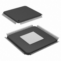
Pin Diagram www.national.com SCAN12100 (Top View) 100–Pin TQFP with Exposed Ground Pad Order Number SCAN12100TYA See NS Number VXF100B 2 20209502 ...
Page 3
Pin Descriptions Pin # Pin Name I/O, Type HIGH SPEED DIFFERENTIAL I/O 12 DOUTP O, CML 11 DOUTN 18 RINP I, CML 17 RINN PARALLEL DATA BUS 65 DIN [0] I, LVTTL or 1.8V 66 DIN [1] LVCMOS Internal 67 ...
Page 4
Pin # Pin Name I/O, Type 79 CDET O, LVTTL or 1.8V LVCMOS CONTROL PINS 82 PE [0] I, LVTTL or 1. [1] LVCMOS Internal pull down 88 EQ [0] I, LVTTL or 1. [1] LVCMOS ...
Page 5
Pin # Pin Name I/O, Type 96 SPMODE [0] I, LVTTL or 1.8V 97 SPMODE [1] LVCMOS Internal pull down 98 TENBMODE I, LVTTL or 1.8V LVCMOS, Internal pull down 99 LOOP [0] I, LVTTL or 1.8V 100 LOOP [1] ...
Page 6
Pin # Pin Name I/O, Type GROUND DAP 101 GND I, Ground Note: I= input O = output Internal pull down = input pin is pulled low by an internal resistor resistor www.national.com Description Device ground. Pad must be soldered ...
Page 7
... Absolute Maximum Ratings If Military/Aerospace specified devices are required, please contact the National Semiconductor Sales Office/ Distributors for availability and specifications. Supply Voltage (AV ) DD18 Supply Voltage (PV , IOV ) DD DD Supply Voltage (AV ) DD33 LVCMOS Input Voltage LVCMOS Output Voltage MDC/MDIO/ADD[0:4],VSEL Input Voltage −0.3V to (AV ...
Page 8
Symbol Parameter V Low level output voltage OL C Input/Output Capacitance IO MDIO/MDC/ADD0-4 DC SPECIFICATIONS V High level input voltage IH V Low level input voltage IL I Input Current IN V High level output voltage OH V Low level ...
Page 9
Symbol Parameter R Output Return Loss Serial data output transition time R F (Notes 11, 15) JIT Serial data output deterministic jitter T-DJ (Notes 3, 11) JIT Serial data output total jitter (Notes T-TJ 3, 11) ...
Page 10
Symbol Parameter Output data transition time R F CDET OUTPUT TIMING SPECIFICATIONS (Read Mode RXCLKMODE=1) t CDET Propagation Delay PDCD CDET OUTPUT TIMING SPECIFICATIONS (Write Mode RXCLKMODE=0) (Note 5) t Setup Time S-C t Hold Time H-C ...
Page 11
Note 1: “Absolute Maximum Ratings” are the ratings beyond which the safety of the device cannot be guaranteed. They are not meant to imply that the device should be operated at these limits. Note 2: Typical parameters are measured at ...
Page 12
AC Timing Diagrams www.national.com READ MODE 20209509 WRITE MODE 20209510 12 ...
Page 13
Functional Description POWER UP AND LINK SYNCHRONIZATION An internal power on reset (POR) circuit disables the trans- mitter output and sets receiver ROUT[9:0], LOS, LOCKB, and CDET in static high state for approximately 150 ms (150ms is based on an ...
Page 14
Reset Type Initial power up ≥ TXPWDNB and RXPWDNB low for ≥ RESETB low for 1 us Write “0” to MDIO RESETB register SPMODE change ≥ TXCLK missing for 7 cycles ≥ RXCLK missing for 7 cycles (Read Mode) TRSTB ...
Page 15
DCM. Pin Type RXCLK (write mode) 1.8V CMOS or LVTTL SYSCLK LVDS SYSCLK can be used to synchronize remote radio heads since it provides a local 30.72 MHz internal ...
Page 16
TRANSMIT DATA DIN[9:0] Transmit Parallel Input Data Transmit input data pins DIN[9:0] are latched on both rising and falling edges of TXCLK. By using both TXCLK edges, the Tx Input 10-bit Mode (TENBMODE = 1) DIN[0] Coded Data Bit DIN[1] ...
Page 17
Transmitter Reset Options TXPWDNB Tx PLL Missing REFCLK 1 Missing TXCLK 1 Not Locked 1 Locked 1 Locked 1 Locked 1 Not Locked RECEIVE DATAPATH Receive Serial Data Input The receive input (RIN) pins are terminated with ...
Page 18
Rx Output 10-bit Mode (TENBMODE = 1) ROUT[3] ROUT[4] ROUT[5] ROUT[6] ROUT[7] ROUT[8] ROUT[9] TABLE 11. Receiver Output Truth Table (10-bit Mode, TENBMODE = 1) RXPWDNB Rx PLL Missing REFCLK & in 10B mode 1 Not Locked ...
Page 19
SYSCLK AND RE REMOTE RADIO HEAD SYNCHRONIZATION The SCAN12100 has independent transmit and receive PLLs as well as an internal ~30.72 MHz oscillator for seamless RE synchronization. Once the SCAN12100 locks to incoming CPRI data, SysCLK becomes phase locked to ...
Page 20
OPMODE 0 (BTS Mode) The LOS mechanism affects the ROUT[9:0] and RXCLK out- puts of the device under 8-bit mode. Upon power up, the ROUT[9:0] and RXCLK pins will be static. Once LOS is low, the device will send data ...
Page 21
IEEE 1149.1 (JTAG) and 1149.6 Operation The SCAN12100 supports a fully compliant IEEE 1149.1 in- terface. The Test Access Port (TAP) provides access to boundary scan cells at single-ended pins for interconnect testing. The TAP also provides access to the ...
Page 22
MDIO Serial Control Interface The MDIO serial control interface allows communication be- tween a station management controller and SCAN12100 de- vices. MDIO and MDC pins are 3.3V LVTTL compliant, not 1.2V compatiable (see Electrical Characteristics table for de- tailed information). ...
Page 23
A normal write operation use the <01>. The data is latched in the SCAN12100 on each edge of the MDC clock. MDIO is sourced from the station side of the MDIO control interface. FIGURE 7. Typical MDIO/MDC Read Operation FIGURE ...
Page 24
Register Description The SCAN12100 implements the device (0x3D.) Other registers defined by 802.3ae-2002 are not implement SCAN12100. The SCAN12100 has a rich MDIO register set to allow the chip to be controlled and monitored through ...
Page 25
... SCAN12100 into a low power mode. Access Bit Description RO National Semiconductor identifier assigned by the IEEE. Access Bit Description RO National Semiconductor identifier assigned by the IEEE. RO SCAN12100 device identifier (3Dh). RO SCAN12100 revision number. Access Bit Description — Reserved for future use. Returns undefined value when read. ...
Page 26
Transmit De-Emphasis Address: 06h Value: 2000h Bit Default Bit Name D15–D8 8'h20 Hyperframe Size D7-D2 6'd0 Reserved D1-D0 2'b00 TX DE 4.1.7 Loopback Mode Address: 07h Value: 0000h Bit Default Bit Name D15–D4 12'h000 Reserved D3-D0 4'b0000 Loopback 4'b0000 ...
Page 27
Speed Mode Address: 0Ah Value: 0000h Bit Default Bit Name D15–D2 14'd0 Reserved D1-D0 2'd0 SPMODE 4.1.11 BIST Status Address: 0Bh Value: 0100h Bit Default Bit Name D15-D13 3'd0 Reserved D12 1'b1 BIST Stopped D11 1'b0 BIST Error D10 ...
Page 28
Loss of Signal (LOS) Address: 11h Value: 0000h Bit Default Bit Name D15–D9 7'd0 Reserved D8 0'b0 LOS Status D7-D0 8'd0 LOS Count 4.1.16 Deserializer Loss of Lock Address: 12h Value: 0000h Bit Default Bit Name D15–D8 8'd0 Reserved ...
Page 29
Misc Status 2 Address: 14h Value: 0000h Bit Default Bit Name D15–D8 8'd0 Reserved D7 RXCDR Lock - Ready D6-D2 Reserved D1 TXPLL Lock - Ready D0 TXPLL Counter 4.1.19 Start of Hyperframe Character Address: 15h Value: 01BCh Bit ...
Page 30
DCM Address: 19h Value: 0000h Bit Default Bit Name D15-D12 4'h0 Reserved D11 1'b0 Hyperframe Length Enable D10-D9 2'b00 Initial Power up wait cycle 2'b00 2'b01 2'b10 2'b11 D8-D1 7'd0 Reserved D0 1'b0 Enable DCM 4.1.24 Reserved Address: 1Ah ...
Page 31
Tser Lower Address 22h Value: 0000h Bit Default Bit Name D15–D0 16'd0 Tser Lower 4.1.30 Tser Upper Address 23h Value: 0000h Bit Default Bit Name D15–D6 10'd0 Reserved D5 1'd0 Reserved D4–D0 5'd0 Tser Upper 4.1.31 Tdes Lower Address ...
Page 32
... This high-speed operation is achieved without significant layout and overall PCB design constraints. However, adhering to a few specific layout guide- lines will optimize signal integrity and performance. The fol- lowing list of topics is covered in National Semiconductor AN-1463. www.national.com Access ...
Page 33
Physical Dimensions inches (millimeters) unless otherwise noted 100-Pin TQFP with Exposed Ground Pad (Top View) See www.national.com/quality/marking_conventions.html for additional part marking information Order Number SCAN12100TYA NS Package Number VXF100B 33 www.national.com ...
Page 34
... For more National Semiconductor product information and proven design tools, visit the following Web sites at: Products Amplifiers www.national.com/amplifiers Audio www.national.com/audio Clock Conditioners www.national.com/timing Data Converters www.national.com/adc Displays www.national.com/displays Ethernet www.national.com/ethernet Interface www.national.com/interface LVDS www.national.com/lvds Power Management www.national.com/power Switching Regulators www.national.com/switchers LDOs www ...