CLC020BCQ/NOPB National Semiconductor, CLC020BCQ/NOPB Datasheet
CLC020BCQ/NOPB
Specifications of CLC020BCQ/NOPB
*CLC020BCQ/NOPB
CLC020BCQ
Available stocks


Related parts for CLC020BCQ/NOPB


CLC020BCQ/NOPB Summary of contents
Page 1
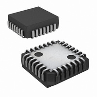
... The device is packaged in a JEDEC 28-lead PLCC. Typical Application © 2003 National Semiconductor Corporation Features n SMPTE 259M serial digital video standard compliant n No external serial data rate setting or VCO filtering components required ...
Page 2
Block Diagram Connection Diagram www.national.com 10091702 28-Pin PLCC Order Number CLC020BCQ See NS Package Number V28A 2 10091701 ...
Page 3
... Absolute Maximum Ratings If Military/Aerospace specified devices are required, please contact the National Semiconductor Sales Office/ Distributors for availability and specifications. Supply Voltage (V − CMOS/TTL Input Voltage ( CMOS/TTL Output Voltage ( CMOS/TTL Input Current (single input −0. +0. Input Current, Other Inputs CMOS/TTL Output Source/Sink Current ...
Page 4
AC Electrical Characteristics Over Supply Voltage and Operating Temperature ranges, unless otherwise specified (Note 3). Symbol Parameter t Hold time HLD L Output inductance GEN R Output resistance GEN Note 1: “Absolute Maximum Ratings” are those parameter values beyond which ...
Page 5
Test Loads (Continued) Timing Diagram FIGURE 2. Test Circuit FIGURE 3. Setup and Hold Timing 5 10091704 10091705 www.national.com ...
Page 6
Device Operation The CLC020 SMPTE 259M Digital Video Serializer is used in digital video signal origination and processing equipment: cameras, video tape recorders, telecines, video test equip- ment and others. It converts parallel component or compos- ite digital video signals ...
Page 7
Device Operation (Continued) BUILT-IN SELF-TEST (BIST) The CLC020 has a built-in self-test (BIST) function. The BIST performs a comprehensive go-no-go test of the device. The test uses either a full-field color bar for NTSC or a PLL pathological for PAL ...
Page 8
Device Operation (Continued) FIGURE 6. Test Pattern Generator Control Sequence TABLE 1. BIST and Test Pattern Generator Control Functions Standard Frame NTSC 4x3 Flat-field black NTSC 4x3 PLL pathological NTSC 4x3 EQ pathological NTSC 4x3 Color bars, 75%, 8-bars (modified, ...
Page 9
Pin Descriptions Pin # Name PCLK 14 Lock Detect 15 V SSO 16 ...
Page 10
Application Information A typical application circuit for the CLC020 is shown in Figure 7. This circuit demonstrates the capabilities of the CLC020 and allows its evaluation in a variety of configura- tions. An assembled demonstration board with more com- prehensive ...
Page 11
... FIGURE 8. SD020EVK Schematic Diagram The jitter test setup used to obtain values quoted in the data sheet consists of: • National Semiconductor SD020EVK, CLC020 evaluation kit • Tektronix TG2000 signal generation platform with DVG1 option • Tektronix VM700T Option 1S Video Measurement Set • ...
Page 12
Application Information is ground). Configure the SD020EVK to operate in the NTSC colour bars, BIST mode. Configure the VM700T to make the jitter measurement in the jitter FFT mode at the frame rate with 1kHz filter bandwidth and Hanning window. ...
Page 13
Application Information PCB LAYOUT AND POWER SYSTEM BYPASS RECOMMENDATIONS Circuit board layout and stack-up for the CLC020 should be designed to provide noise-free power to the device. Good layout practice also will separate high frequency or high level inputs and ...
Page 14
Application Information values. New layouts using the CLC020 will benefit from the greatly reduced ancilliary component count and more com- pact layout. The CLC020 does not require external VCO filtering compo- nents. The external VCO filtering components at pin 17 ...
Page 15
... NATIONAL’S PRODUCTS ARE NOT AUTHORIZED FOR USE AS CRITICAL COMPONENTS IN LIFE SUPPORT DEVICES OR SYSTEMS WITHOUT THE EXPRESS WRITTEN APPROVAL OF THE PRESIDENT AND GENERAL COUNSEL OF NATIONAL SEMICONDUCTOR CORPORATION. As used herein: 1. Life support devices or systems are devices or systems which, (a) are intended for surgical implant ...