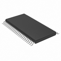
MAX9213EUM+D Maxim Integrated Products, MAX9213EUM+D Datasheet

MAX9213EUM+D
Specifications of MAX9213EUM+D
Related parts for MAX9213EUM+D
MAX9213EUM+D Summary of contents
Page 1
... PLL CLOCK TxCLK GENERATOR Pin Configurations appear at end of data sheet. ________________________________________________________________ Maxim Integrated Products For pricing, delivery, and ordering information, please contact Maxim Direct at 1-888-629-4642, or visit Maxim’s website at www.maxim-ic.com. Programmable DC-Balanced ♦ Programmable DC-Balanced or Non-DC-Balanced Operation ♦ DC Balance Allows AC-Coupling for Ground-Shift Tolerance ♦ ...
Page 2
Programmable DC-Balanced 21-Bit Serializers ABSOLUTE MAXIMUM RATINGS V to GND ...........................................................-0.5V to +4.0V CC LVDS Outputs (TxOUT_, TxCLK OUT_) to GND ...-0.5V to +4.0V 5V Tolerant LVTTL/LVCMOS Inputs (TxIN_, TxCLK IN, PWRDWN) to GND ..............-0.5V to +6.0V (DCB/NC) to GND ...
Page 3
DC ELECTRICAL CHARACTERISTICS (continued) = 100Ω ±1%, PWRDWN = high, DCB/NC = high or low, unless otherwise noted. Typical values are +3.0V to +3.6V +3.3V +25°C.) (Notes ...
Page 4
Programmable DC-Balanced 21-Bit Serializers AC ELECTRICAL CHARACTERISTICS = 100Ω ±1 +3.0V to +3.6V are +3.3V +25°C.) (Notes PARAMETER SYMBOL LVDS Low-to-High Transition Time LVDS High-to-Low ...
Page 5
AC ELECTRICAL CHARACTERISTICS (continued) = 100Ω ±1 +3.0V to +3.6V are +3.3V +25°C.) (Notes PARAMETER SYMBOL TxCLK IN High Time TxCLK IN Low Time TxIN ...
Page 6
Programmable DC-Balanced 21-Bit Serializers = 100Ω ±1 5pF, PWRDWN = high +3.3V WORST-CASE PATTERN AND PRBS SUPPLY CURRENT vs. FREQUENCY 120 MAX9213 DC-BALANCED MODE 100 WORST-CASE PATTERN ...
Page 7
PIN TSSOP TQFN 44, 45, 47, 48, 38, 39, 41, 42, 43 11, 17, 24 11, 18, 40 10, 12, ...
Page 8
Programmable DC-Balanced 21-Bit Serializers TxOUT_- OR TxCLK OUT- TxOUT_+ OR TxCLK OUT+ ΔVOS = |VOS(+) - VOS(-)| (TxOUT_+) - (TxOUT_-) OR (TxCLK OUT+) - (TxCLK OUT-) Figure 1. LVDS Output DC Parameters Figure 2. Worst-Case Test Pattern TxOUT_+ OR TxCLK ...
Page 9
TxCLK OUT (DIFFERENTIAL) CYCLE TxOUT2 TxIN15 (SINGLE ENDED) TxOUT1 TxIN8 (SINGLE ENDED) TxOUT0 TxIN1 (SINGLE ENDED) TPPos0 TPPos1 TPPos2 TPPos3 TPPos4 TPPos5 TPPos6 Figure 5. Non-DC-Balanced Mode LVDS Output Pulse Position Measurement Detailed Description The MAX9209 operates ...
Page 10
Programmable DC-Balanced 21-Bit Serializers TxCLK OUT (DIFFERENTIAL) CYCLE TxOUT2 DCA2 DCB2 (SINGLE ENDED) TxOUT1 DCA1 DCB1 (SINGLE ENDED) TxOUT0 DCA0 DCB0 (SINGLE ENDED) TPPos0 TPPos1 TPPos2 TPPos3 TPPos4 TPPos5 TPPos6 TPPos7 TPPos8 Figure 6. DC-Balanced Mode LVDS ...
Page 11
PWRDWN V CC TxCLK IN TxOUT_, TxCLK OUT HIGH-Z Figure 9. PLL Set Time PWRDWN TxCLK IN TxOUT_, TxCLK OUT Figure 10. Power-Down Delay TxCLK OUT+ TxCLK OUT- CYCLE DCA2 DCB2 TxIN20 TxIN19 TxIN18 TxOUT2 DCA1 DCB1 ...
Page 12
Programmable DC-Balanced 21-Bit Serializers TxCLK OUT+ TxCLK OUT- CYCLE TxIN15 TxIN14 TxIN20 TxIN19 TxIN18 TxOUT2 TxIN8 TxIN7 TxIN13 TxIN12 TxIN11 TxOUT1 TxIN1 TxIN6 TxIN5 TxIN0 TxOUT0 Figure 12. Non-DC-Balanced Mode Inputs Mapped to LVDS Outputs MAX9209 MAX9213 ...
Page 13
MAX9209 MAX9213 2):1 7 TxIN (7 + 2): 2):1 PWRDWN PLL TxCLK IN 21:3 SERIALIZER Figure 14. Two Capacitors per Link, AC-Coupled, DC-Balanced Mode Common-mode voltage differences may be due to ground potential variation ...
Page 14
Programmable DC-Balanced 21-Bit Serializers MAX9209 MAX9213 2):1 7 TxIN (7 + 2): 2):1 PWRDWN PLL TxCLK IN 21:3 SERIALIZER Figure 15. Four Capacitors per Link, AC-Coupled, DC-Balanced Mode Applications Information Selection of AC-Coupling Capacitors ...
Page 15
R = output resistance (Ω) O Equation 1 is for two series capacitors (Figure 14). The bit time ( the period of the parallel clock divided The DSV is 10. See equation 3 for four ...
Page 16
Programmable DC-Balanced 21-Bit Serializers The MAX9209/MAX9213 ESD tolerance is rated for IEC 61000-4-2, Human Body Model and ISO 10605 stan- dards. IEC 61000-4-2 and ISO 10605 specify ESD toler- ance for electronic systems. The IEC 61000-4-2 discharge components are C ...
Page 17
TOP VIEW TxIN4 TxIN5 3 TxIN6 4 GND 5 TxIN7 6 TxIN8 TxIN9 9 MAX9209 MAX9213 TxIN10 10 GND 11 TxIN11 12 TxIN12 TxIN13 15 TxIN14 16 GND ...
Page 18
Programmable DC-Balanced 21-Bit Serializers (The package drawing(s) in this data sheet may not reflect the most current specifications. For the latest package outline information go to www.maxim-ic.com/packages.) N MARKING AAA TOP VIEW ...
Page 19
For the latest package outline information go to www.maxim-ic.com/packages.) ______________________________________________________________________________________ Programmable DC-Balanced 21-Bit Serializers Package Information (continued) 19 ...
Page 20
Programmable DC-Balanced 21-Bit Serializers (The package drawing(s) in this data sheet may not reflect the most current specifications. For the latest package outline information go to www.maxim-ic.com/packages.) 20 ______________________________________________________________________________________ Package Information (continued) ...
Page 21
... Maxim cannot assume responsibility for use of any circuitry other than circuitry entirely embodied in a Maxim product. No circuit patent licenses are implied. Maxim reserves the right to change the circuitry and specifications without notice at any time. Maxim Integrated Products, 120 San Gabriel Drive, Sunnyvale, CA 94086 408-737-7600 ____________________ 21 © 2007 Maxim Integrated Products ...


