MAX3681EAG+ Maxim Integrated Products, MAX3681EAG+ Datasheet
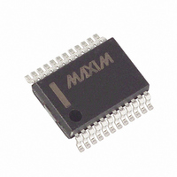
IC 1:4 DESERIALIZR W/LVDS 24SSOP

MAX3681EAG+

Manufacturer Part Number
MAX3681EAG+
Description
IC 1:4 DESERIALIZR W/LVDS 24SSOP
Manufacturer
Maxim Integrated Products
Datasheet

Specifications of MAX3681EAG+

Function
Deserializer
Data Rate
622Mbps
Input Type
LVDS
Output Type
LVDS
Number Of Inputs
1
Number Of Outputs
4
Voltage - Supply
3 V ~ 3.6 V
Operating Temperature
-40°C ~ 85°C
Mounting Type
Surface Mount
Package / Case
24-SSOP
Maximum Operating Temperature
+ 85 C
Minimum Operating Temperature
- 40 C
Mounting Style
SMD/SMT
Operating Supply Voltage
3.3 V
Lead Free Status / RoHS Status
Lead free / RoHS Compliant
The MAX3681 deserializer is ideal for converting
622Mbps serial data to 4-bit-wide, 155Mbps parallel
data in ATM and SDH/SONET applications. Operating
from a single +3.3V supply, this device accepts PECL
serial clock and data inputs, and delivers low-voltage
differential-signal (LVDS) clock and data outputs for
interfacing with high-speed digital circuitry. It also pro-
vides an LVDS synchronization input that enables data
realignment and reframing.
The MAX3681 is available in the extended-industrial
temperature range (-40°C to +85°C), in a 24-pin SSOP
package.
_________________General Description
__________________________Applications
19-1091; Rev 1; 5/04
___________________________________________________________________Typical Operating Circuit
For pricing, delivery, and ordering information, please contact Maxim/Dallas Direct! at
1-888-629-4642, or visit Maxim’s website at www.maxim-ic.com.
PHOTODIODE
MAX3664
622Mbps SDH/SONET Transmission Systems
622Mbps ATM/SONET Access Nodes
Add/Drop Multiplexers
Digital Cross Connects
*REQUIRED ONLY IF OVERHEAD CIRCUIT DOES NOT INCLUDE INTERNAL INPUT TERMINATION.
THIS SYMBOL REPRESENTS A TRANSMISSION LINE OF CHARACTERISTIC IMPEDANCE Z
PREAMP
________________________________________________________________ Maxim Integrated Products
V
CC
= +3.3V
100Ω
1:4 Deserializer with LVDS Outputs
MAX3675
LIMITING
AMP
+3.3V, 622Mbps, SDH/SONET
RECOVERY
CLOCK
DATA
AND
130Ω
130Ω
82Ω
82Ω
♦ Single +3.3V Supply
♦ 622Mbps Serial to 155Mbps Parallel Conversion
♦ 265mW Power
♦ LVDS Data Outputs and Synchronization Inputs
♦ Synchronization Input for Data Realignment and
♦ Differential 3.3V PECL Clock and Data Inputs
________________Ordering Information
______________________________Features
+Denotes Lead Free Package
Pin Configuration appears at end of data sheet.
V
V
MAX3681EAG
MAX3681EAG+
CC
CC
Reframing
= +3.3V
= +3.3V
0
PART
= 50Ω.
82Ω
82Ω
130Ω
130Ω
SCLK+
SCLK-
SD+
SD-
MAX3681
-40°C to +85°C
-40°C to +85°C
TEMP RANGE
GND
V
CC
SYNC+
PCLK+
SYNC-
PCLK-
PD3+
PD2+
PD1+
PD0+
PD3-
PD2-
PD1-
PD0-
V
CC
100Ω*
100Ω*
100Ω*
100Ω*
100Ω*
= +3.3V
24 SSOP
24 SSOP
PIN-PACKAGE
TERMINATION
OVERHEAD
1

Related parts for MAX3681EAG+

MAX3681EAG+ Summary of contents

Page 1

... LVDS Data Outputs and Synchronization Inputs ♦ Synchronization Input for Data Realignment and Reframing ♦ Differential 3.3V PECL Clock and Data Inputs ________________Ordering Information PART MAX3681EAG MAX3681EAG+ +Denotes Lead Free Package Pin Configuration appears at end of data sheet +3.3V CC 130Ω ...

Page 2

SDH/SONET 1:4 Deserializer with LVDS Outputs ABSOLUTE MAXIMUM RATINGS Terminal Voltage (with respect to GND) V ...........................................................................-0. PECL Inputs (SD+/-, SCLK+/-).................................V LVDS Inputs (SYNC+/-)............................................V Output Current, LVDS Outputs (PCLK+/-, PD_+/-) .............10mA Stresses beyond those listed ...

Page 3

Deserializer with LVDS Outputs __________________________________________Typical Operating Characteristics (V = +3.0V to +3.6V, differential loads = 100Ω, unless otherwise noted.) CC MAXIMUM SERIAL CLOCK FREQUENCY vs. TEMPERATURE 2.0 1 3. 3.0V CC 1.4 1.2 ...

Page 4

SDH/SONET 1:4 Deserializer with LVDS Outputs ______________________________________________________________Pin Description PIN NAME +3.3V Supply Voltage CC 3 SD+ Noninverting PECL Serial Data Input. Data is clocked on the SCLK signal’s positive transition. 4 SD- ...

Page 5

Deserializer with LVDS Outputs SCLK D1 SYNC PCLK D4- PD3 PD2 D3- D2- PD1 PD0 D1- NOTE: SIGNALS SHOWN ARE DIFFERENTIAL. FOR EXAMPLE, SCLK = (SCLK+) - (SCLK-). Figure 2. Functional Timing Diagram SCLK SD PCLK ...

Page 6

SDH/SONET 1:4 Deserializer with LVDS Outputs Low-Voltage Differential-Signal (LVDS) Inputs and Outputs The MAX3681 features LVDS inputs and outputs for interfacing with high-speed digital circuitry. The LVDS standard is based on the IEEE 1596.3 LVDS specifica- tion. This ...

Page 7

Deserializer with LVDS Outputs __________________Pin Configuration TOP VIEW SD+ 3 SD- 4 MAX3681 SCLK+ 6 SCLK GND 9 SYNC+ 10 SYNC SSOP ...

Page 8

... Maxim cannot assume responsibility for use of any circuitry other than circuitry entirely embodied in a Maxim product. No circuit patent licenses are implied. Maxim reserves the right to change the circuitry and specifications without notice at any time. 8 ___________________Maxim Integrated Products, 120 San Gabriel Drive, Sunnyvale, CA 94086 (408) 737-7600 © 1996 Maxim Integrated Products INCHES ...

Related keywords