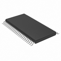
MAX9246EUM+TD Maxim Integrated Products, MAX9246EUM+TD Datasheet

MAX9246EUM+TD
Specifications of MAX9246EUM+TD
Related parts for MAX9246EUM+TD
MAX9246EUM+TD Summary of contents
Page 1
... MAX9254 Falling Yes Pin Configuration appears at end of data sheet. ________________________________________________________________ Maxim Integrated Products For pricing, delivery, and ordering information, please contact Maxim Direct at 1-888-629-4642, or visit Maxim’s website at www.maxim-ic.com. ♦ Programmable ±4%, ±2%, or OFF Spread-Spectrum Output for Reduced EMI ♦ Programmable DC-Balanced or Non-DC-Balanced Modes ♦ ...
Page 2
Deserializers with Programmable Spread Spectrum and DC Balance ABSOLUTE MAXIMUM RATINGS (All voltages referenced to GND LVDSV , PLLV .......................................-0.5V to +4. ......................................................................-0.5V to +6.0V CCO RxIN__, RxCLKIN_.................................................-0.5V to +4.0V PWRDWN ..............................................................-0.5V to ...
Page 3
Deserializers with Programmable Spread Spectrum and DC Balance DC ELECTRICAL CHARACTERISTICS (continued LVDSV = PLLV = +3.0V to +3.6V low, differential input voltage | 0.05V to 1.2V, input common-mode voltage V ...
Page 4
Deserializers with Programmable Spread Spectrum and DC Balance DC ELECTRICAL CHARACTERISTICS (continued LVDSV = PLLV = +3.0V to +3.6V low, differential input voltage | 0.05V to 1.2V, input common-mode voltage V ...
Page 5
Deserializers with Programmable Spread Spectrum and DC Balance AC ELECTRICAL CHARACTERISTICS (continued LVDSV = PLLV = +3.0V to +3.6V DCB = high or low, differential input voltage |V otherwise noted. Typical values are ...
Page 6
Deserializers with Programmable Spread Spectrum and DC Balance FAIL-SAFE IN2 COMPARATOR RxIN_ + OR RxIN_ + OR RxCLKIN+ RxCLKIN 0. IN1 IN1 R R IN1 IN1 RxIN_ - OR RxIN_ - ...
Page 7
Deserializers with Programmable Spread Spectrum and DC Balance RCOP 2.0V 2.0V RxCLKOUT 0.8V RCOH RSRC 2.0V RxOUT_ 0.8V Figure 5b. Falling-Edge Output Setup/Hold and High/Low Times RCIP + RxCLKIN_ RCCD RxCLKOUT 1.5V Figure 6b. ...
Page 8
Deserializers with Programmable Spread Spectrum and DC Balance SSG RxCLKIN_ RxCLKOUT RxOUT_ TIMING SHOWN FOR FALLING-EDGE STROBE (MAX9244/MAX9246/MAX9254) PWRDWN = HIGH Figure 9. Phase-Locked-Loop Set Time from SSG Change FREQUENCY SSM f (MAX) RxCLKOUT f RxCLKIN_ ...
Page 9
Deserializers with Programmable Spread Spectrum and DC Balance (V = PLLV = LVDSV = V = +3.3V CCO voltage V = 1.2V +25°C, MAX9244/MAX9254, unless otherwise noted WORST-CASE AND PRBS SUPPLY ...
Page 10
Deserializers with Programmable Spread Spectrum and DC Balance (V = PLLV = LVDSV = V = +3.3V CCO voltage V = 1.2V +25°C, MAX9244/MAX9254, unless otherwise noted RxCLKOUT POWER SPECTRUM vs. ...
Page 11
Deserializers with Programmable Spread Spectrum and DC Balance PIN NAME 1 RxOUT17 Channel 2 Single-Ended Outputs 2 RxOUT18 3, 25, 32, GND Ground 38 RxOUT19 Channel 2 Single-Ended Outputs 5 RxOUT20 Three-Level-Logic, Spread-Spectrum Generator Control Input. SSG ...
Page 12
Deserializers with Programmable Spread Spectrum and DC Balance PIN NAME 34 RxOUT7 35 RxOUT8 37 RxOUT9 Channel 1 Single-Ended Outputs 39 RxOUT10 40 RxOUT11 41 RxOUT12 Digital Supply Voltage. Bypass pin as possible. 43 RxOUT13 ...
Page 13
Deserializers with Programmable Spread Spectrum and DC Balance Detailed Description The MAX9242/MAX9244/MAX9246/MAX9254 deserialize three LVDS serial-data inputs into 21 single-ended LVC- MOS/LVTTL outputs. The outputs are programmable for no spread or for a spread of ±2% or ±4%, relative ...
Page 14
Deserializers with Programmable Spread Spectrum and DC Balance + - RxCLKIN_ CYCLE DCA2 DCB2 TxIN20 TxIN19 TxIN18 RxIN2_ DCA1 DCB1 TxIN13 TxIN12 TxIN11 RxIN1_ DCA0 TxIN6 TxIN5 TxIN4 DCB0 RxIN0_ TxIN_, DCA_, AND DCB_ ARE DATA ...
Page 15
Deserializers with Programmable Spread Spectrum and DC Balance ±4% OR ±2% SPREAD SSG RxCLKOUT RxOUT_ Figure 13. Output Waveforms when Spread Amount is Changed SSG NO SPREAD RxCLKOUT RxOUT_ Figure 14. Output Waveforms when Spread is Added ±4% OR ...
Page 16
Deserializers with Programmable Spread Spectrum and DC Balance INTERNAL PLL1 LOCK INTERNAL SSPLL LOCK RxCLKOUT RxOUT_ Figure 16. Output Waveforms when PLL1 Loses Lock and Locks Again INTERNAL SSPLL LOCK RxCLKOUT RxOUT_ TIMING SHOWN FOR STABLE CLOCK AND DATA ...
Page 17
Deserializers with Programmable Spread Spectrum and DC Balance MAX9209/MAX9213 7 7:1 7 TxIN 7:1 7 7:1 PWRDWN PLL TxCLK IN 21:3 SERIALIZER Figure 18. DC-Coupled Link, Non-DC-Balanced Mode R is required to match the transmission line impedance T (usually ...
Page 18
Deserializers with Programmable Spread Spectrum and DC Balance MAX9209/MAX9213 2):1 7 TxIN (7 + 2): 2):1 PWRDWN PLL TxCLK IN 21:3 SERIALIZER Figure 19. Two Capacitors per Link, AC-Coupled, DC-Balanced Mode The capacitor ...
Page 19
Deserializers with Programmable Spread Spectrum and DC Balance MAX9209/MAX9213 2):1 7 TxIN (7 + 2): 2):1 PWRDWN PLL TxCLK IN 21:3 SERIALIZER Figure 20. Four Capacitors per Link, AC-Coupled, DC-Balanced Mode Link Power-Up ...
Page 20
Deserializers with Programmable Spread Spectrum and DC Balance trace used (microstrip or stripline). Note that two 50Ω PC board traces do not have 100Ω differential imped- ance when brought close together—the impedance goes down when the traces are brought ...
Page 21
Deserializers with Programmable Spread Spectrum and DC Balance SSG and DCB provides the proper mid-level voltage under conditions of low input current. The mid-level input current must not be greater than ±10µA, and the mid-level logic state cannot be ...
Page 22
Deserializers with Programmable Spread Spectrum and DC Balance Ordering Information (continued) PART TEMP RANGE MAX9246EUM -40°C to +85°C MAX9246EUM/V+ -40°C to +85°C MAX9246GUM -40°C to +105°C MAX9246GUM/V+ -40°C to +105°C MAX9254EUM -40°C to +85°C MAX9254EUM/V+ -40°C to +85°C + ...
Page 23
... Maxim cannot assume responsibility for use of any circuitry other than circuitry entirely embodied in a Maxim product. No circuit patent licenses are implied. Maxim reserves the right to change the circuitry and specifications without notice at any time. Maxim Integrated Products, 120 San Gabriel Drive, Sunnyvale, CA 94086 408-737-7600 ____________________ 23 © 2009 Maxim Integrated Products DESCRIPTION Maxim is a registered trademark of Maxim Integrated Products, Inc ...


