PI2EQX5864CZFE Pericom Semiconductor, PI2EQX5864CZFE Datasheet
PI2EQX5864CZFE
Specifications of PI2EQX5864CZFE
Available stocks


Related parts for PI2EQX5864CZFE

PI2EQX5864CZFE Summary of contents
Page 1
... PCIe with Equalization, Emphasis, &I Description Pericom Semiconductor’s PI2EQX5864C is a low power, PCIe compliant signal redriver. The device provides programmable equalization, amplifi cation, and de-emphasis by using 8 select bits, to optimize performance over a variety of physical mediums by reducing Inter-symbol interference. ...
Page 2
Pin Description Pin # Pin Name Data Signals 2 A0RX+, 3 A0RX- 48 A0TX+, 47 A0TX- 7 A1RX+, 8 A1RX- 43 A1TX+, 42 A1TX- 12 A2RX+, 13 A2RX- 38 A2TX+, 37 A2TX- 17 A3RX+, 18 A3RX- 33 A3TX+, 32 A3TX- ...
Page 3
Pin # Pin Name 24 RESET# 50 RXD_A 22 RXD_B 53 SCL 52 SDA 55, 56, Center Pad GND 1, 6, 11, 16, 21, 29, VDD 34, 39, 44, 49 DESCRIPTION of OPERATION Confi guration Modes Device confi guration can ...
Page 4
Output Confi guration The PI2EQX5864C provides fl exible output strength and emphasis controls to provide the optimum signal to pre-compensate for losses across long trace or noisy environments so that the receiver gets a clean with good eye opening. Control ...
Page 5
Receiver Detect Automatic Receiver Detection is a feature that can set the number of active channels. By sensing the presence of a load device on the output, the channel can be automatically enabled for operation. This allows the PI2EQX5864C to ...
Page 6
Loopback Operation Each lane of the PI2EQX5864C provides a loopback mode for test purposes which is controlled by a strapping pin and I bit. The LB# pin controls all lanes together. When this pin is high normal data mode is ...
Page 7
Confi guration Register Summary Byte Mnemonic Function 0 SIG Signal Detect, indicates valid input signal level 1 RX50 Receiver Detect Output, indicates whether a receiver load was detected Loopback and Emphasis Control, provides for control of the loopback function and ...
Page 8
MOS-FET’s in table 1 are suitable to be used as level shifter. The 2SK3018 are low cost devices and have good properties for 1.2V/3.3V level shifting, isolation and protection. Manufacturer Manufac- Part Number turer 2SK3018T106 Rohm Transferring Data Every byte ...
Page 9
Acknowledge Data transfer with acknowledge is required from the master. When the master releases the SDA line (HIGH) during the acknowledge clock pulse, the PI2EQX5864C will pull down the SDA line during the acknowledge clock pulse so that it remains ...
Page 10
Byte 2 - Loopback and Emphasis Control Register (LBEC) LB_xyxy#=0=loopback mode, LB_xyxy#=1=normal mode, DE_x=0=pre-emphasis, DE_x=1=de-emphasis Bit 7 6 Name LB_A0B0# LB_A1B1# Type R/W R/W Power-on LB# LB# State Note: R=Read only, W=Write only, R/W=Read and Write, X=Undefi ned, rsvd=reserved for ...
Page 11
BYTE 5 - Channel Reset (RESET) RESET# =0=reset, RESET# =1=normal operation. Latch from RESET# input at startup Bit 7 6 Name RES_A0# RES_B0# Type R/W R/W Power- State Note: R=Read only, W=Write only, R/W=Read and Write, X=Undefi ned, ...
Page 12
The A-Channels Equalizer and Output Control register is used to control the confi guration of the input equalizer and output emphasis and levels of the four A channels. These register bits are loaded from the input confi guration pins of ...
Page 13
I C Data Transfer 1. Read sequence ACK PI2EQX5864C Master DEV SEL 2. Write sequence ACK PI2EQX5864C Master DEV SEL 3. Combined sequence DUMMY BYTE ACK ACK ...
Page 14
Maximum Ratings (Above which useful life may be impaired. For user guidelines, not tested.) Storage Temperature ...................................... Supply Voltage to Ground Potential........ –0.5V to +2.5V DC SIG Voltage....................................... –0. Current Output ........................................ –25mA to +25mA Power Dissipation Continuous ...
Page 15
Equalizer Symbol Parameters J Residual jitter RS-T J Residual jitter RS-D J Random jitter RM Notes 1. K28.7 pattern is applied differentially at point A as shown in AC test circuit (see fi gure). 2. Total jitter does not include ...
Page 16
SDA and SCL I/O for I C-bus (V Symbol Parameters V DC input logic high input logic low output logic low OL V Hysteresis of Schmitt trigger input hys Characteristics of the SDA ...
Page 17
START SDA t SU;DAT LOW SCL t HD;STA t HD;DAT S 09-0002 5.0Gbps 4-Lane PCIe with Equalization, Emphasis and HD;STA t SU;STA HIGH Timing Channel Latency, 5.0 Gbps 17 ...
Page 18
Output Level Settings (1V left, and 0.5V right at 5.0 Gbps) 0.0 dB (Dx = 000) –6.5 dB (Dx = 101) Output De-Emphasis Characteristics 09-0002 5.0Gbps 4-Lane PCIe with Equalization, Emphasis and I –3.5 dB (Dx = 010) –8.5 dB ...
Page 19
Eye Diagrams 5.0Gbps (input left, output right) Data Waveforms, 2.5Gbps (left) & 5.0Gbps (right) Signal Source Connector AC Test Circuit Referenced in the Electrical Characteristic Table 09-0002 5.0Gbps 4-Lane PCIe with Equalization, Emphasis and I FR4 A B SmA SmA ...
Page 20
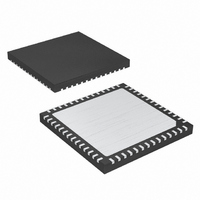
... Packaging Mechanical: 56-Contact TQFN (ZF) 08-0208 Ordering Information Ordering Number PI2EQX5864CZFE Notes: • Thermal characteristics can be found on the company web site at www.pericom.com/packaging/ • Pb-free and Green • X suffi Tape/Reel Pericom Semiconductor Corporation • 1-800-435-2336 • www.pericom.com 09-0002 ReDriver is a trademark of Pericom Semiconductor. ...