PI2EQX5864CZFE Pericom Semiconductor, PI2EQX5864CZFE Datasheet - Page 11
PI2EQX5864CZFE
Manufacturer Part Number
PI2EQX5864CZFE
Description
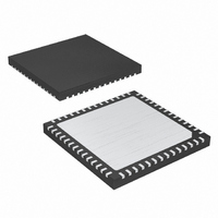
IC PCI-E REDRIVER 56TQFN
Manufacturer
Pericom Semiconductor
Series
ReDriver™r
Type
Redriverr
Datasheet
1.PI2EQX5864CZFE.pdf
(20 pages)
Specifications of PI2EQX5864CZFE
Tx/rx Type
CML
Capacitance - Input
50pF
Voltage - Supply
1.15 V ~ 1.25 V
Current - Supply
800mA
Mounting Type
Surface Mount
Package / Case
56-TQFN
Operating Temperature (min)
0C
Operating Temperature Classification
Commercial
Operating Temperature (max)
70C
Rad Hardened
No
Lead Free Status / RoHS Status
Lead free / RoHS Compliant
Delay Time
-
Lead Free Status / RoHS Status
Lead free / RoHS Compliant, Compliant
Available stocks
Company
Part Number
Manufacturer
Quantity
Price
Company:

Part Number:
PI2EQX5864CZFE
Manufacturer:
Pericom
Quantity:
135
Company:
Part Number:
PI2EQX5864CZFE
Manufacturer:
Pericom
Quantity:
367


BYTE 5 - Channel Reset (RESET)
RESET# =0=reset, RESET# =1=normal operation. Latch from RESET# input at startup
Note: R=Read only, W=Write only, R/W=Read and Write, X=Undefi ned, rsvd=reserved for future use
The Channel Reset register allows for restart of an individual channels Receiver Detect function. A transition from 0 to 1 initiates a
new Receiver Detect cycle (if the channel is enabled and receiver detect is enabled). While static at 0 or 1, the RESET# bit will have
no effect on operation. The Channel Reset bits are read/write allowing the current state to be checked.
BYTE 6 - Power Down Control (PWR)
PD_xy# =0=channel off/power down, PD_xy# =1=normal operation, Latch from PD# input at startup
Note: R=Read only, W=Write only, R/W=Read and Write, X=Undefi ned, rsvd=reserved for future use
The Power Down Control register allows for individual control over each channel for power savings. When PD_xy# is logic 0 the
channel is turned off. When PD_xy# is 1 then the channel is enabled for normal operation.
BYTE 7 - Receiver Detect Enable (RXD)
RXD_xy =0=channel off/power down, RXD_xy =1=normal operation, Latch from PD# input at startup
Note: R=Read only, W=Write only, R/W=Read and Write, X=Undefi ned, rsvd=reserved for future use
The Receiver Detect Enable register allows for control of the receiver detect state machine for each individual channel. When
RXD_xy is set to 0, then the receiver detect function is disabled. When RXD_xy is logic 1, then the receiver detect state machine is
enabled for operation. The initial state of the register bits are determined by the RXD_A and RXD_B input pins during power-up.
BYTE 8 - A-Channels Equalizer and Output Control (AEOC)
SELx_A: Equalizer confi guration, Dx_A: Emphasis control, Sx_A: Output level control (see Confi guration Table)
Note: R=Read only, W=Write only, R/W=Read and Write, X=Undefi ned, rsvd=reserved for future use
Power-on
Power-on
Power-on
Power-on
Name
Name
Name
Name
Type
State
Type
State
Type
State
Type
State
Bit
Bit
Bit
Bit
09-0002
RES_A0#
RXD_A0
PD_A0#
SEL0_A
R/W
R/W
R/W
R/W
7
1
7
1
7
1
7
1
RES_B0#
RXD_B0
PD_B0#
SEL1_A
R/W
R/W
R/W
R/W
6
1
6
1
1
1
6
6
RES_A1#
RXD_A1
PD_A1#
SEL2_A
R/W
R/W
R/W
R/W
5
1
5
1
5
1
5
1
RES_B1#
RXD_B1
PD_B1#
D0_A
R/W
R/W
R/W
R/W
4
1
4
1
11
4
1
4
1
with Equalization, Emphasis and I
RES_A2#
RXD_A2
PD_A2#
D1_A
R/W
R/W
R/W
R/W
3
1
3
1
3
1
3
1
5.0Gbps 4-Lane PCIe
RES_B2#
RXD_B2
PD_B2#
D2_A
R/W
R/W
R/W
R/W
2
1
2
1
2
1
2
1
RES_A3#
RXD_A3
PD_A3#
S0_A
R/W
R/W
R/W
R/W
®
1
1
1
1
1
1
1
1
2.0 ReDdriver™
PS8934D
PI2EQX5864C
2
C Control
RES_B3#
RXD_B3
PD_B3#
S1_A
R/W
R/W
R/W
R/W
0
1
0
1
0
1
0
1
07/08/09
Related parts for PI2EQX5864CZFE
Image
Part Number
Description
Manufacturer
Datasheet
Request
R

Part Number:
Description:
Fast CMOS bus interface register
Manufacturer:
Pericom Semiconductor
Datasheet:
Part Number:
Description:
4-bit,4-port bus exchange switch
Manufacturer:
Pericom Semiconductor
Datasheet:
Part Number:
Description:
Manufacturer:
Pericom Semiconductor
Datasheet:
Part Number:
Description:
Manufacturer:
Pericom Semiconductor
Datasheet:
Part Number:
Description:
Manufacturer:
Pericom Semiconductor
Datasheet:
Part Number:
Description:
Manufacturer:
Pericom Semiconductor
Datasheet:
Part Number:
Description:
Manufacturer:
Pericom Semiconductor
Datasheet:
Part Number:
Description:
Manufacturer:
Pericom Semiconductor
Datasheet:
Part Number:
Description:
Manufacturer:
Pericom Semiconductor
Datasheet:
Part Number:
Description:
Manufacturer:
Pericom Semiconductor
Datasheet:
Part Number:
Description:
Manufacturer:
Pericom Semiconductor
Datasheet:
Part Number:
Description:
Manufacturer:
Pericom Semiconductor
Datasheet:
Part Number:
Description:
Manufacturer:
Pericom Semiconductor
Datasheet:
Part Number:
Description:
Manufacturer:
Pericom Semiconductor
Datasheet: