LX5255CPW Microsemi Analog Mixed Signal Group, LX5255CPW Datasheet
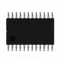
IC TERM SCSI 9LINE LVD 24TSSOP

LX5255CPW

Manufacturer Part Number
LX5255CPW
Description
IC TERM SCSI 9LINE LVD 24TSSOP
Manufacturer
Microsemi Analog Mixed Signal Group
Type
SCSI, LVDr
Datasheet

Specifications of LX5255CPW

Number Of Terminations
9
Voltage - Supply
2.7 V ~ 5.25 V
Operating Temperature
0°C ~ 70°C
Mounting Type
Surface Mount
Package / Case
28-TSSOP
Lead Free Status / RoHS Status
Contains lead / RoHS non-compliant

Available stocks

Company
Part Number
Manufacturer
Quantity
Price
Part Number:
LX5255CPW
Manufacturer:
SANYO
Quantity:
5
Part Number:
LX5255CPW
Manufacturer:
MSC
Quantity:
20 000
Copyright © 2000
Rev. 1.1, 2006-02-27
Differential
designed to comply with the LVD
termination specification in the SPI-4
document. The LX5255 is specifically
designed for LVD only applications.
Because the LX5255 supports only
LVD, it has lower output capacitance
than multimode terminators such as
the LX5250.
standard
individual high bandwidth drivers
maximize channel separation, reduce
channel-to-channel noise and cross
talk to insure Ultra320 performance.
Differential Sense (DIFSENS) pin
IMPORTANT: For the most current data, consult MICROSEMI’s website: http://www.microsemi.com
When the LX5255 is enabled, the
The LX5255 is a Low Voltage
The LX5255 utilizes an industry
L X 5255
TM
LVD
(LVD)
architecture.
11861 Western Avenue, Garden Grove, CA. 92841, 714-898-8121, Fax: 714-893-2570
+
terminator
D E S C R I P T I O N
-
The
Note: Available in Tape & Reel. Append the letters “TR” to the
supplies a voltage between 1.2V and
1.4V. In application, the terminator
DIFFB input is connected to the system
DIFSENS line. If there are no single
ended or High Voltage Differential
(HVD) devices attached to the system,
the LVD output will be enabled. If the
DIFSENS line is LOW, indicating a
single ended device, the LX5255 output
will be HiZ. If the DIFSENS line is
HIGH, indicating a HVD device, the
LX5255 output will be HiZ.
sleep/disable mode. Applying a logic
HIGH to the DISC pin puts the LX5255
in sleep mode. During sleep mode,
power dissipation is reduced to a meager
5μA while also placing all outputs and
the DIFSENS function in a HiZ state.
The LX5255 has a TTL compatible
T Y P I C A L A P P L I C A T I O N
0 to 70
T
LX5255 Typical Application
A
Integrated Products Division
(°C)
PACKAGE ORDER INFO
part number. (i.e. LX5255CPW-TR)
®
Microsemi
PW
RoHS Compliant / Pb-free
Transition DC: 0442
LX5255CPW
Plastic TSSOP
24-Pin
9-Line LVD SCSI Terminator
P
RODUCTION DATA SHEET
+
Compliant with SPI-2 (Ultra2),
SPI-3 (Ultra160), and SPI-4
(Ultra320)
2.5pF Maximum Disabled Output
Capacitance
Fast Response, No External
Capacitors Required
5µA Supply Current in Disconnect
Mode
30mA Supply During Normal
Operation
Logic Command Disconnects All
Termination Lines
DIFSENS Line Driver
Current Limit and Thermal
Protection
Pin Compatible With Unitrode
UCC5640
-
K E Y F E A T U R E S
L X 5255
LX5255
Page 1

Related parts for LX5255CPW

LX5255CPW Summary of contents

Page 1

... T (°C) A RoHS Compliant / Pb-free Transition DC: 0442 LX5255CPW Note: Available in Tape & Reel. Append the letters “TR” to the part number. (i.e. LX5255CPW-TR) Microsemi Integrated Products Division LX5255 Compliant with SPI-2 (Ultra2), SPI-3 (Ultra160), and SPI-4 (Ultra320) 2.5pF Maximum Disabled Output ...

Page 2

Term Power (V )............................................................................................-0. TERM Signal Line Voltage .............................................................................................-0. Differential Voltage .............................................................................................-0.3V to ...

Page 3

TM Unless otherwise specified, the following specifications apply over the operating ambient temperature 0°C and DISCONNECT = 0V. Parameter LVD Terminator Section VTerm Supply Current Common Mode Voltage Offset Voltage (Note 1) Differential Terminator Impedance Common Mode Impedance Output Capacitance ...

Page 4

... Comp. + LVD POWER ON & MODE DELAY Figure 1 – LX5255CPW Block Diagram ESCRIPTION Negative signal termination lines for LVD mode. Positive signal termination lines for LVD mode. Power supply pin for terminator. Connect to SCSI bus VTERM. Must be decoupled by one 4.7 F low-ESR capacitor for every three terminator devices µ ...

Page 5

TM HOST TERMPOWER VTERM LX5255 DISCONNECT DISC GND NC* Pin 1 4.7uF 4.7uF VTERM LX5255 DISC GND NC* Pin 1 4.7uF VTERM LX5255 DISC GND NC* Pin 1 4.7uF * The capacitor on Pin 1 can be placed on the ...

Page 6

TM PW 24-Pin Thin Small Shrink Outline (TSSOP) E SEATING PLANE * Lead Coplanarity Note: 1. Dimensions do not include mold flash or protrusions; these shall not exceed 0.155mm(.006”) on any side. Lead dimension shall not include solder coverage. Copyright ...

Page 7

TM PRODUCTION DATA – Information contained in this document is proprietary to Microsemi and is current as of publication date. This document may not be modified in any way without the express written consent of Microsemi. Product processing does not ...

Related keywords