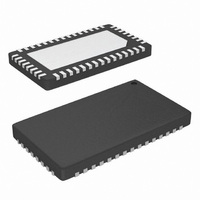
ISL36411DRZ-T7 Intersil, ISL36411DRZ-T7 Datasheet - Page 8

ISL36411DRZ-T7
Manufacturer Part Number
ISL36411DRZ-T7
Description
IC EQUALIZER REC 11.3GBPS 46QFN
Manufacturer
Intersil
Series
QLx™r
Datasheet
1.ISL36411DRZ-T7.pdf
(12 pages)
Specifications of ISL36411DRZ-T7
Applications
Data Transport
Voltage - Supply
1.1 V ~ 1.3 V
Package / Case
46-WQFN
Mounting Type
Surface Mount
Rohs Compliant
Yes
Lead Free Status / RoHS Status
Lead free / RoHS Compliant
Interface
-
Other names
ISL36411DRZ-TS-TR
ISL36411DRZ-TS-TR
QLX411RIQT7
QLX411RIQT7-TR
QLX411RIQT7-TR
ISL36411DRZ-TS-TR
QLX411RIQT7
QLX411RIQT7-TR
QLX411RIQT7-TR
Available stocks
Company
Part Number
Manufacturer
Quantity
Price
Company:
Part Number:
ISL36411DRZ-T7
Manufacturer:
Intersil
Quantity:
283
Part Number:
ISL36411DRZ-T7
Manufacturer:
INTERSIL
Quantity:
20 000
ISL36411 CML Input and Output Buffers
The input and output buffers for the high-speed data
channels in the ISL36411 are implemented using CML
(shown in Figures 4 and 5).
LINE SILENCE/QUIESCENT MODE
Line silence is commonly broken by the limiting
amplification in other equalizers. This disruption can be
detrimental in many systems that rely on line silence as
part of the protocol. The ISL36411 contains special lane
management capabilities to detect and preserve periods
of line silence while still providing the fidelity-enhancing
benefits of limiting amplification during active data
transmission. Line silence is detected by measuring the
amplitude of the equalized signal and comparing that to
a threshold set by the voltage at the DT pin. When the
amplitude falls below the threshold, the output driver
stages are muted and held at their nominal common
mode voltage
1. The output common mode voltage remains constant during both active data transmission and output muting modes
FIGURE 5. CML OUTPUT EQUIVALENT CIRCUIT
IN[N]
IN[P]
FIGURE 4. CML INPUT EQUIVALENT CIRCUIT
1
.
V
DD
50O
50O Ω
Ω
8
1
Stage
st
Filter
ISL36411
LOS Bar Indicator
Pins LOSB[k] are used to output the state of the muting
circuitry to serve as a loss of signal indicator for channel
k. This signal is directly derived from the muting signal
off the DT-threshold signal detector output. The LOS
signal goes LOW when the power signal is below the DT
threshold and HIGH when the power goes above the DT
threshold. This feature is meant to be used in optical
systems (e.g. QSFP) where there are no quiescent or
electrical-idle states. In these cases, the DT threshold is
used to determine the sensitivity of the LOS indicator.
Detection Thereshold (DT) Pin Functionality
The ISL36411 is capable of maintaining periods of line
silence by monitoring the channel for loss of signal (LOS)
conditions and subsequently muting the output driver
when such a condition is detected. A reference voltage
applied to the detection threshold (DT) pins is used to set
the LOS threshold of the internal signal detection
circuitry (one pin for a pair of channels). The DT voltage
is set with an external pull-up resistor, RDT. For typical
applications, a 15kΩ resistor is recommended for
channels with loss greater than 12dB at 5GHz, and a
0.9kΩ resistor is recommended for lower loss channels.
Other values of the resistor may also be applicable;
therefore DT settings should be verified on an
application-specific basis.
PCB Layout Considerations
Because of the high speed of the ISL36411 signals,
careful PCB layout is critical to maximize performance.
The following guidelines should be adhered to as closely
as possible:
• All high speed differential pair traces should have a
• Avoid using vias for high speed traces as this will
• Input and output traces need to have DC blocking
• For each differential pair, the positive trace and the
• Maintain a constant solid ground plane underneath
• Each VDD pin should be connected to 1.2V and also
• If 4 channels of the device are set to the same boost,
characteristic impedance of 50Ω with respect to
ground plane and 100Ω with respect to each other.
create discontinuity in the traces’ characteristic
impedance.
capacitors (100nF). Capacitors should be placed as
close to the chip as possible.
negative trace need to be of the same length in order
to avoid intra-pair skew. A Serpentine technique may
be used to match trace lengths.
the high-speed differential traces.
bypassed to ground through a 10nF and a 100pF
capacitor in parallel. Minimize the trace length and
avoid vias between the VDD pin and the bypass
capacitors in order to maximize the power supply
noise rejection.
then the quantity of CP resistors can be reduced by
tying both CP pins together.
March 25, 2010
FN6965.1


