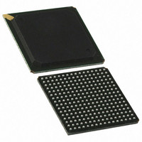
PI7C9X20505GPBNDE Pericom Semiconductor, PI7C9X20505GPBNDE Datasheet - Page 30

PI7C9X20505GPBNDE
Manufacturer Part Number
PI7C9X20505GPBNDE
Description
IC PCIE PACKET SWITCH 256BGA
Manufacturer
Pericom Semiconductor
Series
GreenPacket™r
Specifications of PI7C9X20505GPBNDE
Applications
Data Transport
Interface
Advanced Configuration Power Interface (ACPI)
Package / Case
256-PBGA
Mounting Type
Surface Mount
Lead Free Status / RoHS Status
Lead free / RoHS Compliant
Voltage - Supply
-
Available stocks
Company
Part Number
Manufacturer
Quantity
Price
Company:
Part Number:
PI7C9X20505GPBNDE
Manufacturer:
Pericom
Quantity:
180
June 2009 – Revision 1.5
Pericom Semiconductor
ADDRESS
54h
56h
58h
60h
62h
64h
66h
68h
70h
72h
74h
76h
78h
80h
82h
84h
86h
88h
90h
92h
94h
15Ch (Port 2)
15Ch: Bit [22:16]
160h: Bit [7:0]
15Ch (Port 3)
15Ch: Bit [22:16]
160h: Bit [7:0]
15Ch (Port 4)
15Ch: Bit [22:16]
160h: Bit [7:0]
214h (Port 0)
214h: Bit [7:0]
214h: Bit [9:8]
214h: Bit [14:13]
218h: Bit [0]
214h (Port 1)
214h: Bit [7:0]
214h: Bit [9:8]
214h: Bit [14:13]
218h: Bit [0]
214h (Port 2)
214h: Bit [7:0]
214h: Bit [9:8]
214h: Bit [14:13]
218h: Bit [0]
214h (Port 3)
214h: Bit [7:0]
214h: Bit [9:8]
214h: Bit [14:13]
218h: Bit [0]
214h (Port 4)
214h: Bit [7:0]
214h: Bit [9:8]
214h: Bit [14:13]
218h: Bit [0]
B0h (Port 0)
B0h: Bit [15:0]
B0h (Port 1)
B0h: Bit [15:0]
B0h (Port 2)
B0h: Bit [15:0]
B0h (Port 3)
B0h: Bit [15:0]
B0h (Port 4)
B0h: Bit [15:0]
B0h (Port 0)
B0h: Bit [31:16]
B0h (Port 1)
B0h: Bit [31:16]
B0h (Port 2)
B0h: Bit [31:16]
B0h (Port 3)
B0h: Bit [31:16]
B0h (Port 4)
B0h: Bit [31:16]
B4h (Port 0)
B4h: Bit [31:16]
B4h (Port 1)
B4h: Bit [31:16]
B4h (Port 2)
B4h: Bit [31:16]
PCI CFG
OFFSET
DESCRIPTION
VC1 MAX Time Slot and TC/VC Map for Port 2
VC1 MAX Time Slot and TC/VC Map for Port 3
VC1 MAX Time Slot and TC/VC Map for Port 4
Power Budget Register for Port 0
Power Budget Register for Port 1
Power Budget Register for Port 2
Power Budget Register for Port 3
Power Budget Register for Port 4
Replay Time-out Counter for Port 0
Replay Time-out Counter for Port 1
Replay Time-out Counter for Port 2
Replay Time-out Counter for Port 3
Replay Time-out Counter for Port 4
Acknowledge Latency Timer for Port 0
Acknowledge Latency Timer for Port 1
Acknowledge Latency Timer for Port 2
Acknowledge Latency Timer for Port 3
Acknowledge Latency Timer for Port 4
PHY Parameter for Port 0
PHY Parameter for Port 1
PHY Parameter for Port 2
Page 30 of 81
Bit [6:0]: The maximum time slot supported by VC1
Bit [15:8]: When set, it indicates the corresponding TC is
mapped into VC1
Bit [6:0]: The maximum time slot supported by VC1
Bit [15:8]: When set, it indicates the corresponding TC mapped
into VC1
Bit [6:0]: The maximum time slot supported by VC1
Bit [15:8]: When set, it indicates the corresponding TC is
mapped into VC1
Bit [7:0]: Base Power
Bit [9:8]: Data Scale
Bit [11:10]: PM State
Bit [15]: System Allocated
Bit [7:0]: Base Power
Bit [9:8]: Data Scale
Bit [11:10]: PM State
Bit [15]: System Allocated
Bit [7:0]: Base Power
Bit [9:8]: Data Scale
Bit [11:10]: PM State
Bit [15]: System Allocated
Bit [7:0]: Base Power
Bit [9:8]: Data Scale
Bit [11:10]: PM State
Bit [15]: System Allocated
Bit [7:0]: Base Power
Bit [9:8]: Data Scale
Bit [11:10]: PM State
Bit [15]: System Allocated
Bit [15:0]: Relay Time-out Counter
Bit [15:0]: Relay Time-out Counter
Bit [15:0]: Relay Time-out Counter
Bit [15:0]: Relay Time-out Counter
Bit [15:0]: Relay Time-out Counter
Bit [31:16]: Acknowledge Latency Timer
Bit [31:16]: Acknowledge Latency Timer
Bit [31:16]: Acknowledge Latency Timer
Bit [31:16]: Acknowledge Latency Timer
Bit [31:16]: Acknowledge Latency Timer
Bit [31:16]: PHY Parameter
Bit [31:16]: PHY Parameter
Bit [31:16]: PHY Parameter
5Port-5Lane PCI Express Switch
GreenPacket
PI7C9X20505GP
Datasheet
TM
Family


