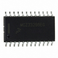
MCZ33298EG Freescale Semiconductor, MCZ33298EG Datasheet - Page 9

MCZ33298EG
Manufacturer Part Number
MCZ33298EG
Description
IC SWITCH 8X LOSIDE W/SPI 24SOIC
Manufacturer
Freescale Semiconductor
Datasheet
1.MCZ33298EGR2.pdf
(28 pages)
Specifications of MCZ33298EG
Applications
*
Interface
*
Voltage - Supply
*
Package / Case
24-SOIC (7.5mm Width)
Mounting Type
Surface Mount
Lead Free Status / RoHS Status
Lead free / RoHS Compliant
Available stocks
Company
Part Number
Manufacturer
Quantity
Price
Company:
Part Number:
MCZ33298EG
Manufacturer:
RENESAS
Quantity:
2 000
Part Number:
MCZ33298EG
Manufacturer:
FREESCALE
Quantity:
20 000
Part Number:
MCZ33298EGR2
Manufacturer:
FREESCALE
Quantity:
20 000
.
Table 7. Dynamic Electrical Characteristics
Typical values noted reflect the approximate parameter mean at T
Analog Integrated Circuit Device Data
Freescale Semiconductor
POWER OUTPUT TIMING
DIGITAL INTERFACE TIMING
Notes
Output Rise Time (V
Output Fall Time (V
Output Turn ON Delay Time (V
Output Turn-OFF Delay Time (V
Output Short Fault Disable Report Delay
Output OFF Fault Report Delay
SCLK Clock Period
SCLK Clock High Time
SCLK Clock Low Time
Required Low State Duration for Reset (V
Falling Edge of CS to Rising Edge of SCLK (Required Setup Time)
Falling Edge of SCLK to Rising Edge of CS (Required for Setup Time)
SI to Falling Edge of SCLK (Required for Setup Time)
Falling Edge of SCLK to SI (Required for Hold Time)
SO Rise Time (C
SO Fall Time (C
SI, CS, SCLK, Incoming Signal Rise Time
SI, CS, SCLK, Incoming Signal Fall Time
Time from Falling Edge of CS to SO Low-impedance
Time from Rising Edge of CS to SO High-impedance
Time from Rising Edge of SCLK to SO Data Valid
29.
30.
31.
32.
33.
34.
35.
36.
37.
38.
39.
Characteristics noted under conditions 4.5V
SFPD = 0.2 x V
SFPD = 0.2 x V
0.2V
Output Rise and Fall time respectively measured across a 26Ω resistive load at 10 to 90 percent, and 90 to 10 percent voltage points.
Output Turn ON Delay time measured from 50 percent rising edge of CS to 90 percent of Output OFF voltage (V
resistive load.
Output Turn OFF Delay time measured from 50 percent rising edge of CS to 10 percent of Output OFF voltage (V
resistive load.
Output Short Fault Delay time measured from rising edge of CS to I
V
Output OFF Fault Report Delay measured from 50 percent rising edge of CS to rising edge of output. See Figure 9.
Clock period include 75ns rise plus 75ns fall transition in addition to clock high and low time.
RST Low duration measured with outputs enabled and going to OFF or disabled condition.
Rise and Fall time of incoming SI, CS, and SCLK signals suggested for design consideration to prevent the occurrence of double pulsing.
Time required for output status data to be available for use at the SO pin.
Time required for output status data to be terminated at the SO pin.
Time required to obtain valid data out from SO following the rise of SCLK. See Figure 5.
DD
DD
. See Figures 8 and 10.
< SO > 0.8V
L
L
= 200pF)
DD
DD
= 200pF)
(34)
PWR
PWR
DD
= 13V, R
= 13V, R
, C
L
Characteristic
= 200pF
PWR
(33)
PWR
L
L
= 26Ω)
= 26Ω)
= 13V, R
= 13V, R
DYNAMIC ELECTRICAL CHARACTERISTICS
(32)
(36)
IL
(36)
(29)
(29)
< 0.2V
L
L
= 26Ω)
= 26Ω)
(39)
DD
≤
(37)
(38)
V
)
(30)
(35)
(31)
DD
≤
5.5V, 9.0V
A
≤
OUT
= 25°C under nominal conditions, unless otherwise noted.
V
PWR
-= 2.0A point with output ON, V
t
t
t
t
t
t
Symbol
DLY(OFF)
t
DLY(OFF)
WSCLKH
SI(HOLD)
t
DLY(ON)
WSCLKL
t
t
≤
t
DLY(SF)
SO(DIS)
W(RST)
SO(EN)
t
PSCLK
t
t
VALID
t
t
t
LEAD
SISU
t
RSO
t
16V, -40°C
LAG
FSO
RSI
FSI
t
t
R
F
DYNAMIC ELECTRICAL CHARACTERISTICS
≤
Min
500
175
175
250
250
250
125
125
0.4
0.4
1.0
1.0
25
25
—
—
—
—
—
—
—
T
A
≤
ELECTRICAL CHARACTERISTICS
125°C, unless otherwise noted.
OUT
Typ
1.5
2.5
5.0
5.0
50
50
50
50
50
25
25
25
25
50
—
—
—
—
—
—
—
= 5.0V, and SFPD = 0.2
PWR
PWR
) with R
Max
100
100
200
200
200
200
125
) with R
20
20
15
15
75
75
—
—
—
—
—
—
—
—
L
L
= 26Ω
= 26Ω
Unit
µs
µs
µs
µs
µs
µs
ns
ns
ns
ns
ns
ns
ns
ns
ns
ns
ns
ns
ns
ns
ns
33298
9


