ADG508AKNZ Analog Devices Inc, ADG508AKNZ Datasheet
ADG508AKNZ
Specifications of ADG508AKNZ
Available stocks


Related parts for ADG508AKNZ


ADG508AKNZ Summary of contents
Page 1
FEATURES 44 V supply maximum rating analog signal range SS DD Single-/dual-supply specifications Wide supply range: 10 16.5 V Extended plastic temperature range: −40°C to +85°C Low power dissipation maximum Low leakage: 20 ...
Page 2
ADG508A/ADG509A TABLE OF CONTENTS Features .............................................................................................. 1 Functional Block Diagrams ............................................................. 1 General Description ......................................................................... 1 Product Highlights ........................................................................... 1 Revision History ............................................................................... 2 Specifications ..................................................................................... 3 Dual Supply ................................................................................... 3 Single Supply ................................................................................. 5 REVISION HISTORY 7/09—Rev ...
Page 3
SPECIFICATIONS DUAL SUPPLY −10 −16.5 V, unless otherwise noted Table 1. ADG508A/ ADG509A K Version Parameter +25°C ANALOG SWITCH Analog Signal Range ...
Page 4
ADG508A/ADG509A ADG508A/ ADG509A K Version Parameter +25°C C (Off ) (Off ) D ADG508A 22 ADG509A Charge Injection 4 INJ POWER SUPPLY I 0 Power Dissipation 10 1 Sample tested ...
Page 5
SINGLE SUPPLY GND = 0 V, unless otherwise noted Table 2. ADG508A/ ADG509A K Version Parameter +25°C ANALOG SWITCH Analog Signal Range GND 500 ON 700 ...
Page 6
ADG508A/ADG509A ADG508A/ ADG509A K Version Parameter +25°C POWER SUPPLY I 0.6 DD Power Dissipation 10 1 Sample tested at 25°C to ensure compliance. ADG508A/ ADG508A/ ADG509A ADG509A B Version T Version −40°C to −40°C to +85°C +25°C +85°C +25°C 0.6 ...
Page 7
ABSOLUTE MAXIMUM RATINGS T = 25°C, unless otherwise noted. A Table 3. Parameter Ratings GND GND – Analog Inputs Voltage ...
Page 8
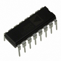
ADG508A/ADG509A PIN CONFIGURATIONS AND FUNCTION DESCRIPTIONS ADG508A GND TOP VIEW (Not to Scale ...
Page 9
ADG509A TOP VIEW S1A 4 13 (Not to Scale) S2A 5 12 S3A 6 11 S4A Figure 6. ADG509A DIP, SOIC Table 6. ADG509A Pin ...
Page 10
ADG508A/ADG509A TYPICAL PERFORMANCE CHARACTERISTICS The multiplexers are guaranteed functional with reduced single or dual supplies down to 4.5 V. 700 600 500 SS 400 300 V = +10. –10.8V SS 200 V = +15V ...
Page 11
TEST CIRCUITS Note: All digital input signal rise and fall times measured from 10 Figure 14 ...
Page 12
ADG508A/ADG509A 3V 0V 50% t OPEN 3V 50 (EN × ΔV INJ ADDRESS A2 DRIVE ( 50Ω ...
Page 13
SINGLE-SUPPLY OCTAL DAC APPLICATION The following circuit shows the ADG508A connected as a demulti- plexer to provide eight separate, digitally programmable voltages ( from the AD7245A. The AD7245A is a complete 12-bit, voltage output DAC with ...
Page 14
ADG508A/ADG509A OUTLINE DIMENSIONS 0.210 (5.33) MAX 0.150 (3.81) 0.130 (3.30) 0.115 (2.92) 0.022 (0.56) 0.018 (0.46) 0.014 (0.36) 0.200 (5.08) 0.200 (5.08) 0.125 (3.18) 0.800 (20.32) 0.790 (20.07) 0.780 (19.81 0.280 (7.11) 0.250 (6.35) 1 0.240 (6.10) 8 ...
Page 15
BSC 1.75 (0.0689) 0.25 (0.0098) 1.35 (0.0531) 0.10 (0.0039) COPLANARITY SEATING 0.51 (0.0201) 0.10 PLANE 0.31 (0.0122) COMPLIANT TO JEDEC STANDARDS MS-012-AC ...
Page 16
... ADG508A/ADG509A ORDERING GUIDE Model Temperature Range ADG508AKN −40°C to +85°C 1 ADG508AKNZ −40°C to +85°C ADG508AKR −40°C to +85°C ADG508AKR-REEL −40°C to +85°C ADG508AKR-REEL7 −40°C to +85°C 1 ADG508AKRZ −40°C to +85°C 1 ADG508AKRZ-REEL −40°C to +85°C ...