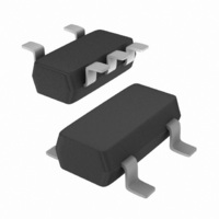
74HCT1G66GV,125 NXP Semiconductors, 74HCT1G66GV,125 Datasheet - Page 3

74HCT1G66GV,125
Manufacturer Part Number
74HCT1G66GV,125
Description
IC SWITCH SPST SC74A
Manufacturer
NXP Semiconductors
Series
74HCTr
Datasheet
1.74HC1G66GW125.pdf
(18 pages)
Specifications of 74HCT1G66GV,125
Function
Switch
Circuit
1 x SPST- NO
Voltage Supply Source
Single Supply
Voltage - Supply, Single/dual (±)
4.5 V ~ 5.5 V
Operating Temperature
-40°C ~ 125°C
Mounting Type
Surface Mount
Package / Case
SC-74A, SOT-753
Lead Free Status / RoHS Status
Lead free / RoHS Compliant
Other names
74HCT1G66GV
74HCT1G66GV
935271886125
74HCT1G66GV
935271886125
NXP Semiconductors
7. Functional description
Table 4.
[1]
8. Limiting values
Table 5.
In accordance with the Absolute Maximum Rating System (IEC 60134). Voltages are referenced to GND (ground = 0 V).
[1]
[2]
9. Recommended operating conditions
Table 6.
Voltages are referenced to GND (ground = 0 V).
[1]
74HC_HCT1G66_4
Product data sheet
Input E
L
H
Symbol
V
I
I
I
I
I
T
P
Symbol Parameter
V
V
V
T
IK
SK
SW
CC
GND
stg
amb
t/ V
CC
tot
CC
I
SW
H = HIGH voltage level; L = LOW voltage level.
The input and output voltage ratings may be exceeded if the input and output current ratings are observed.
For TSSOP5 and SC-74A packages: above 87.5 C the value of P
To avoid drawing V
exceed 0.4 V. If the switch current flows into pin Z, no V
drop across the switch, but the voltage at pins Y and Z may not exceed V
supply voltage
input voltage
switch voltage
ambient temperature
input transition rise
and fall rate
Function table
Limiting values
Recommended operating conditions
Parameter
supply voltage
input clamping current
switch clamping current
switch current
supply current
ground current
storage temperature
total power dissipation
CC
current out of pin Z, when switch current flows in pin Y, the voltage drop across the bidirectional switch must not
[1]
Conditions
V
V
V
V
CC
CC
CC
CC
= 2.0 V
= 4.5 V
= 6.0 V
= 10.0 V
Conditions
V
V
V
T
I
I
SW
amb
< 0.5 V or V
< 0.5 V or V
[1]
Rev. 04 — 19 December 2008
> 0.5 V or V
= 40 C to +125 C
CC
current will flow out of terminal Y. In this case there is no limit for the voltage
I
I
> V
> V
Switch
OFF
ON
SW
tot
Min
2.0
0
0
40
-
-
-
-
CC
derates linearly with 4.0 mW/K.
CC
< V
74HC1G66; 74HCT1G66
+ 0.5 V
74HC1G66
+ 0.5 V
CC
CC
or GND.
1.67
Typ
+25
+ 0.5 V
5.0
-
-
-
-
-
Single-pole single-throw analog switch
+125
Max
10.0
V
V
625
139
83
35
CC
CC
[1]
[1]
[2]
Min
4.5
Min
-
-
-
-
-
0
0
40
-
-
-
-
0.5
50
65
74HCT1G66
1.67
Typ
+25
5.0
-
-
-
-
-
Max
+11.0
50
-
+150
250
© NXP B.V. 2008. All rights reserved.
20
20
25
+125
Max
V
V
139
5.5
CC
CC
-
-
-
Unit
V
mA
mA
mA
mA
mA
mW
C
Unit
V
V
V
ns/V
ns/V
ns/V
ns/V
C
3 of 18


