AC101LKQT Broadcom, AC101LKQT Datasheet
AC101LKQT
Specifications of AC101LKQT
Available stocks


Related parts for AC101LKQT


AC101LKQT Summary of contents
Page 1
Ultra Low-Power 10/100 Ethernet Transceiver with Auto-MDIX The AC101L is a single channel, low power, 10/100BASE-TX/FX transceiver. The AC101L transceiver has an integrated voltage regulator to allow operation from ...
Page 2
... Added input voltage high and low values (all digital input pins). Updated FX application figure and Power and ground filtering figure. Initial release. Altima Communications, Inc. A Fully Owned Subsidiary of Broadcom Corporation P.O. Box 57013 16215 Alton Parkway Irvine, California 92619-7013 © ...
Page 3
Section 1: Functional Description...................................................................................... 1 Encoder/Decoder ......................................................................................................................................... 1 Link Monitor .................................................................................................................................................. 1 Carrier Sense (CRS)/RXDV .......................................................................................................................... 2 Collision Detection ....................................................................................................................................... 2 Auto-Negotiation .......................................................................................................................................... 2 Parallel Detection ......................................................................................................................................... 3 Analog Adaptive Equalizer .......................................................................................................................... 3 Clock Recovery ............................................................................................................................................ 3 Baseline Wander ...
Page 4
AC101L LED Configuration .................................................................................................................................15 LED [3:0] Event Table ...........................................................................................................................15 Section 5: Register Description ....................................................................................... 17 TP PHY Register Summary ........................................................................................................................17 Register 0: Control Register .................................................................................................................18 Register 1: Status Register ...................................................................................................................19 Register 2: PHY Identifier 1 Register ....................................................................................................20 Register 3: PHY ...
Page 5
Section 6: 4B/5B Code Group........................................................................................... 31 Section 7: SMI Read/Write Sequence............................................................................... 33 Section 8: Timing and AC Characteristics ...................................................................... 35 Clock Timing ............................................................................................................................................... 35 Reset Timing ............................................................................................................................................... 35 Management Data Interface timing ........................................................................................................... 36 100BASE-TX/FX MII Transmit System Timing ...
Page 6
AC101L Figure 1: AC101L Functional Block Diagram ....................................................................................................... i Figure 2: AC101L Pinout Diagram ....................................................................................................................11 Figure 3: Reset Timing......................................................................................................................................35 Figure 4: Management Interface Timing ...........................................................................................................36 Figure 5: 100BASE-TX/FX MII Transmit Timing ...............................................................................................37 Figure 6: 100BASE-T MII Receive Timing ........................................................................................................39 Figure ...
Page 7
Table 1: Pinout and Signal Definitions................................................................................................................ 7 Table 2: LED [3:0] Event Table ........................................................................................................................ 15 Table 3: TP PHY Register Summary................................................................................................................ 17 Table 4: Register 0: Control Register ............................................................................................................... 18 Table 5: Register 1: Status Register................................................................................................................. 19 Table 6: ...
Page 8
AC101L Table 33: SMI Read/Write Sequence ...............................................................................................................33 Table 34: Clock Timing .....................................................................................................................................35 Table 35: Reset Timing .....................................................................................................................................35 Table 36: Management Interface Timing ..........................................................................................................36 Table 37: 100BASE-X MII Transmit System Timing .........................................................................................37 Table 38: 100BASE-TX/FX MII Receive System Timing ..................................................................................38 Table ...
Page 9
The AC101L is a single-chip, Fast Ethernet transceiver. It performs all of the physical ...
Page 10
AC101L In 100BASE-FX mode, the external fiber-optic receiver performs the signal energy detection function and communicates this information directly to the SD signal (PIN 28). In 10BASE-T mode, a link pulse detection circuit constantly monitors the RXP/RXN pins for the ...
Page 11
Full-Duplex 4.5/1.11 10BASE ARALLEL ETECTION Because there are many devices in the field that do not support the ANEN process, but must still be communicated with necessary to detect and link ...
Page 12
AC101L TX_CLK. This provides a continuously running RX_CLK. At the PCS interface, the 5-bit data RXD[4:0] is synchronized to the 25 MHz RX_CLK ASELINE ANDER A 100BASE-TX data stream is not always DC balanced. Because the receive ...
Page 13
FEF ( AULT Auto-negotiation provides the mechanism to inform the link partner that a remote fault has occurred. Auto-negotiation is disabled, however, in the 100BASE-FX applications. An alternative in-band signaling function (FEFI) is used to ...
Page 14
AC101L MAC I NTERFACE MII The Media Independent Interface (MII 18-wire MAC/PHY interface described in IEEE 802.3u. The purpose of the interface is to allow MAC layer devices to attach to a variety of physical layer devices through ...
Page 15
Section 2: Pin Des cr iptions Many of the pin have multiple functions. The multifunction pins are designated by bold style of the pin number. The separate descriptions of these pins are listed in the proper sections. Designers must ...
Page 16
AC101L PIN # PIN name Type 16 REPEATER/ CRS GND G 18 VCC P 19 PHYAD0/INTR BURNIN/LED0 SPD100/LED1 DUPLEX/LED2 ANEN/LED3 PDOWN B ...
Page 17
PIN # PIN name Type 42 RST I 43 MDIO B 44 MDC PHYAD1/ RXD3 B 46 PHYAD2/ RXD2 B 47 PHYAD3/ RXD1 B 48 PHYAD4/ RXD0 B Document AC101L-DS05-R Table 1: Pinout and Signal Definitions ...
Page 18
AC101L Page 10 Preliminary Data Sheet B roa dcom 03/10/03 Document AC101L-DS05-R ...
Page 19
iag VCC GND RXDV RX_CLK RXER GND VCC TXER TXC TXEN TXD0 TXD1 Document AC101L-DS05 AC101L 6 ...
Page 20
AC101L Page 12 Preliminary Data Sheet B roa dcom 03/10/03 Document AC101L-DS05-R ...
Page 21
rat scr ESET The PHY can be reset in three ways: • During initial power on. • Hardware reset: (See ...
Page 22
AC101L C S LOCK OURCE The clock source for this chip is from the XI pin. In MII mode, it can connect MHz 50 ppm (parts per million) OSC MHz 50 ppm XTAL (crystal). ...
Page 23
The default LED modes are as shown below: LED0 LED1 Link/Activity Speed LED C ONFIGURATION The LEDs are fully configurable to other operational modes. Each LED has two 16-bit registers to define its operation. See “Common Registers” on page ...
Page 24
AC101L Page 16 Preliminary Data Sheet B roa dcom 03/10/03 Document AC101L-DS05-R ...
Page 25
Des cri The first 7 registers of the MII register set are defined by the MII specification. In addition to these required registers ...
Page 26
AC101L EGISTER ONTROL EGISTER Bit Name Description 0.15 Reset 1 = PHY reset. This bit is self-clearing. 0.14 Loopback 1 = Enable loopback mode. This loops back TXD to RXD and ignores all of the activity ...
Page 27
EGISTER TATUS EGISTER Bit Name Description 1.15 100BASE-T4 Permanently tied to zero; indicates no 100BASE-T4 capability. 1.14 100BASE- 100BASE-TX full-duplex capable. Full-Duplex 0 = Not 100BASE-TX full-duplex capable. Default value: SPD100 && DUPLEX ...
Page 28
AC101L R 2: PHY I EGISTER DENTIFIER Bit Name Description 2.[15:0] a Composed of the 3rd through 18th bits of the Organizationally Unique OUI Identifier (OUI), respectively. a. Based on an OUI of 0010A9 (hexadecimal PHY I EGISTER ...
Page 29
EGISTER UTO EGOTIATION P M AGE ESSAGE Table 9: Register 5: Auto-Negotiation Link Partner Ability Register/Link Partner Next Page Message Bit Name Description 5.15 Next Page 1 = Link partner desires a Next Page transfer. ...
Page 30
AC101L EGISTER UTO EGOTIATION Table 11: Register 7: Auto-Negotiation Next Page Transmit Register Bit Name Description 7. Another Next Page desired other Next Page transmit desired. 7.14 Reserved – 7.13 ...
Page 31
R 17 EGISTER NTERRUPT Table 13: Register 17: Interrupt Control/Status Register Bit Name 17.15 Jabber_IE 17.14 RXER_IE 17.13 Page_Rx_IE 17.12 PD_Fault_IE 17.11 LP_Ack_IE 17.10 Link_Status_Change_IE 17.9 R_Fault_IE 17.8 ANEN_Comp_IE 17.7 Jabber_Int 17.6 RXER_Int 17.5 Page_Rx_Int 17.4 PD_Fault_Int ...
Page 32
AC101L R 19 EGISTER OWER OOPBACK Table 15: Register 19: Power/Loopback Register Bit Name Description 19.[14:7] Reserved Reserved 19.6 Reserved Reserved 19.5 Disable 1 = Disables watchdog timer. Watchdog Timer 0 = Enables advanced power saving mode. for ...
Page 33
R 22 EGISTER OWER ANAGEMENT Table 18: Register 22: Power Management Register Bit Name Description 22.[15:14] Reserved – 22.13 PD_PLL 1 = PLL circuit powers down. 22.12 PD_EQUAL 1 = Equalizer circuit powers down. 22.11 PD_BT_RCVR 1 ...
Page 34
AC101L R 24: CRC R EGISTER FOR ECENT Table 20: Register 24: CRC for Recent Received Packet Bit Name Description 24.[15:0] CRC16 Displays CRC16 value. For system-level test purposes OMMON EGISTERS The following registers are mapped to Reg28-31 ...
Page 35
OMMON EGISTER AP TO Table 23: Common Register 4: (Map to Reg. 29, Page 1 A28.[15:12]=0001) LED Blink Rate Bit Name Description A1.29.[15:8] Reserved – A1.29.[7:0] Blink Rate Set LED blink rate. The blink rate ...
Page 36
AC101L OMMON EGISTER EGISTER Default Operation for LED1 is ON when 100 Mbps operation. Table 27: Common Register 8: (Map to Reg. 30, Page 2 A.28.[15:12]=0010) LED1 Setting2 Register Bit Name Description A2.30.[15:8] ...
Page 37
C R 11: (M OMMON EGISTER R EGISTER Default operation for LED3 is BLINK when COL. Table 30: Common Register 11: (Map to Reg. 30, Page 3 A.28[.15:12]=0011) LED3 Setting1 Register Reg.bit Name Description A3.30.[15:13] Reserved – A3.30.12 Force ...
Page 38
AC101L Page 30 Preliminary Data Sheet B roa dcom 03/10/03 Document AC101L-DS05-R ...
Page 39
Se ction 6: 4B/5B Code Group Symbol name 4B code 5B code 0 0000 11110 1 0001 01001 2 0010 10100 3 0011 10101 4 0100 01010 5 0101 01011 6 0110 01110 7 0111 01111 8 1000 10010 ...
Page 40
AC101L Page 32 Preliminary Data Sheet B roa dcom 03/10/03 Document AC101L-DS05-R ...
Page 41
Section 7: SMI Read/Write Sequence SMI read/write sequence – Pream Start (32 bits) (2 bits) Read 1…1 01 Write 1…1 01 Document AC101L-DS05-R Table 33: SMI Read/Write Sequence Opcode PHYAD REGAD (2 bits) (5 bits) (5 bits) 10 AAAAA ...
Page 42
AC101L Page 34 Preliminary Data Sheet B roa dcom 03/10/03 Document AC101L-DS05-R ...
Page 43
Se ction 8: Timing Char acte ristics C T LOCK IMING Parameter XTAL input cycle time XTAL input high/low time XTAL input rise/fall time R T ESET IMING Parameter Reset pulse length low period with stable ...
Page 44
AC101L ANAGEMENT ATA Parameter MDC cycle time MDC high/low MDC rise/fall time MDIO input setup time to MDC rising MDIO input hold time from MDC rising MDIO output delay from MDC rising MDC ) MDIO (Into AC101L ...
Page 45
MII T Table 37: 100BASE-X MII Transmit System Timing Parameter Symbol TX_CLK period tCK TX_CLK high period tCKH TX_CLK low period tCKL TXEN to /J/ tTJ TXEN sampled to CRS tCSA TXEN sampled to COL tCLA !TXEN to ...
Page 46
AC101L 100BASE-TX/FX MII R Parameter RX_CLK period RX_CLK high period RX_CLK low period /J/K to RXDV assert /J/K to CRS assert /J/K to COL assert /T/R to !RXDV /T/R to !CRS /T/R to !COL RX propagation delay RXD[3:0], RXDV assert: ...
Page 47
RX_CLK tRDVA RXDV RXD[3:0] RXER RXDV /J/K RXIP/N FXRP/N tRCSA CRS tRCLA COL tCK tCKH 25Mhz RX_CLK tpLH100 RXD[3:0]; RXDV Valid Data tpHL=invalid tpLH=Output delay Document AC101L-DS05-R Start of Packet tCKL - tCKL Figure 6: 100BASE-T MII ...
Page 48
AC101L 10BASE-T MII T RANSMIT Table 39: 10BASE-T MII Transmit System Timing Parameter SYM TX_CLK period tCK TX_CLK high period tCKH TX_CLK low period tCKL TXEN to SOP tTJ TXEN sampled to CRS tTCSA TXEN sampled to COL tTCLA !TXEN ...
Page 49
MII R ECEIVE Table 40: 10BASE-T MII Receive System Timing Parameter Symbol RX_CLK period tCK RX_CLK high period tCKH RX_CLK low period tCKL SOP to CRS tRCSA SOP to COL tRCLA EOP to !RXDV tRDVD EOP to !CRS ...
Page 50
AC101L tCK tCKH RX_CLK tRDVA RXDV RXD[3:0] RXER RXDV SOP RXIP/N tRCSA CRS tRCLA COL tCK tCKH 25Mhz RX_CLK tpLH10 RXD[3:0]; RXDV Valid Data tpLH=Output delay Page 42 Start of Packet tCKL tCKL Figure 8: 10BASE-T Receive Timing B roa ...
Page 51
C A OPPER PPLICATION TXP AC101L TXN RXP RXN Auto MDI/MDIX Magnetics: BEL: S558-5999-W2; PULSE: H1102; HALO: TG110-S050N2 Document AC101L-DS05-R T ERMINATION Auto MDI/MDIX 1:1 2.5 V 1:1 Figure 9: TX Application B roa dcom RJ45 ...
Page 52
AC101L Page 44 Preliminary Data Sheet B roa dcom 03/10/03 Document AC101L-DS05-R ...
Page 53
Se ction 9: Ele ctrica l Char acte ristics The following electrical characteristics are design goals rather than characterized numbers. Note A M BSOLUTE AXIMUM Parameter Supply voltage Storage temperature Electrostatic discharge Table 42: Current Requirement at 2.5 V ...
Page 54
AC101L R O ECOMMENDED PERATING Table 44: Recommended Operating Conditions Parameter Symbol Pins Ambient operating T – A temperature AC101L Bias voltage V RBIAD BIAS Common mode input V RD± ICM voltage Common mode input V RD± ICM voltage Differential ...
Page 55
Sec cati on Te rmi n ati on 3_3 V 2_5 V RXP RXN SD/FXEN TXP TXN C12 1 µF Document ...
Page 56
AC101L Page 48 Preliminary Data Sheet B roa dcom 03/10/03 Document AC101L-DS05-R ...
Page 57
Pow Grou Place all CAPs as close as possible to each power pin of AC101L 2_5 V ...
Page 58
AC101L Page 50 Preliminary Data Sheet B roa dcom 03/10/03 Document AC101L-DS05-R ...
Page 59
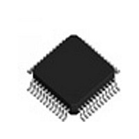
echa nfo rma Document AC101L-DS05-R Figure 12: Quad Flat Pack outline (7×7 mm) B roa dcom Page 51 ...
Page 60
AC101L Page 52 Preliminary Data Sheet B roa dcom 03/10/03 Document AC101L-DS05-R ...
Page 61
Section 13 : The rma l Para mete rs Airflow (feet per minute) ( ° C/W) Theta JA ( ° C/W) at maximum junction temperature of 125 ° C Theta JC Document AC101L-DS05-R Table 45: Thermal parameters 0 100 ...
Page 62
AC101L Page 54 Preliminary Data Sheet B roa dcom 03/10/03 Document AC101L-DS05-R ...
Page 63
... Se ction 14: Orde ring Info rmation Part number AC101LKQT AC101LIQT Document AC101L-DS05-R Package 48TQFP 48TQFP B roa dcom Ambient temperature 0 ° +70 ° C –40 ° +85 ° C Page 55 ...
Page 64
... Altima Communications, Inc. A Fully Owned Subsidiary of Broadcom Corporation ® Broadcom Corporation reserves the right to make changes without further notice to any products or data herein to improve reliability, function, or design. Information furnished by Altima Communications is believed to be accurate and reliable. However, Altima Communications does not assume any liability arising out of the application or use of this information, nor the application or use of any product or circuit described herein, neither does it convey any license under its patent rights nor the rights of others ...