ADG509FBNZ Analog Devices Inc, ADG509FBNZ Datasheet
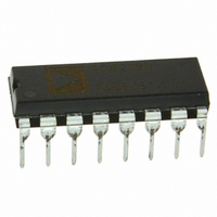
IC MULTIPLEXER DUAL 4X1 16DIP

ADG509FBNZ

Manufacturer Part Number
ADG509FBNZ
Description
IC MULTIPLEXER DUAL 4X1 16DIP
Manufacturer
Analog Devices Inc
Type
Analog Multiplexerr
Datasheet

Specifications of ADG509FBNZ

Function
Multiplexer
Circuit
2 x 4:1
On-state Resistance
400 Ohm
Voltage Supply Source
Single Supply
Voltage - Supply, Single/dual (±)
15V
Current - Supply
0.1µA
Operating Temperature
-40°C ~ 85°C
Mounting Type
Through Hole
Package / Case
16-DIP (0.300", 7.62mm)
No. Of Circuits
2
Supply Current
600µA
On State Resistance Max
300ohm
Supply Voltage Range
10.8V To 16.5V
Operating Temperature Range
-40°C To +85°C
Analog Switch Case Style
DIP
Multiplexer Configuration
Single 4:1
Number Of Inputs
8
Number Of Outputs
2
Number Of Channels
1
Analog Switch On Resistance
350@±15VOhm
Analog Switch Turn On Time
250ns
Analog Switch Turn Off Time
250ns
Package Type
PDIP
Power Supply Requirement
Dual
Single Supply Voltage (min)
Not RequiredV
Single Supply Voltage (typ)
Not RequiredV
Single Supply Voltage (max)
Not RequiredV
Dual Supply Voltage (typ)
±15V
Dual Supply Voltage (max)
±22V
Power Dissipation
3.3mW
Mounting
Through Hole
Pin Count
16
Operating Temp Range
-40C to 85C
Operating Temperature Classification
Industrial
Lead Free Status / RoHS Status
Lead free / RoHS Compliant
Lead Free Status / RoHS Status
Lead free / RoHS Compliant, Lead free / RoHS Compliant

Available stocks

Company
Part Number
Manufacturer
Quantity
Price
Part Number:
ADG509FBNZ
Manufacturer:
MICREL
Quantity:
6 256
Part Number:
ADG509FBNZ
Manufacturer:
ADI
Quantity:
2 500
FEATURES
Low on resistance (300 Ω typical)
Fast switching times
Low power dissipation (3.3 mW maximum)
Fault and overvoltage protection (−40 V to +55 V)
All switches off with power supply off
Analog output of on channel clamped within power
Latch-up proof construction
Break-before-make construction
TTL and CMOS compatible inputs
APPLICATIONS
Existing multiplexer applications (both fault-protected and
New designs requiring multiplexer functions
GENERAL DESCRIPTION
The ADG508F, ADG509F, and ADG528F
multiplexers, with the ADG508F and ADG528F comprising
eight single channels and the ADG509F comprising four
differential channels. These multiplexers provide fault protec-
tion. Using a series n-channel, p-channel, n-channel MOSFET
structure, both device and signal source protection is provided
in the event of an overvoltage or power loss. The multiplexer
can withstand continuous overvoltage inputs from −40 V to
+55 V. During fault conditions, the multiplexer input (or out-
put) appears as an open circuit and only a few nanoamperes of
leakage current will flow. This protects not only the multiplexer
and the circuitry driven by the multiplexer, but also protects
the sensors or signal sources that drive the multiplexer.
The ADG508F and ADG528F switch one of eight inputs to a
common output as determined by the 3-bit binary address lines
A0, A1, and A2. The ADG509F switches one of four differential
inputs to a common differential output as determined by the
2-bit binary address lines A0 and A1. The ADG528F has on-
chip address and control latches that facilitate microprocessor
1
Rev. E
Information furnished by Analog Devices is believed to be accurate and reliable. However, no
responsibility is assumed by Analog Devices for its use, nor for any infringements of patents or other
rights of third parties that may result from its use. Specifications subject to change without notice. No
license is granted by implication or otherwise under any patent or patent rights of Analog Devices.
Trademarks and registered trademarks are the property of their respective owners.
Protected by U.S. Patent No. 5,389, 811.
t
t
supplies if an overvoltage occurs
nonfault-protected)
ON
OFF
250 ns maximum
250 ns maximum
1
are CMOS analog
Fault-Protected Analog Multiplexers
One Technology Way, P.O. Box 9106, Norwood, MA 02062-9106, U.S.A.
Tel: 781.329.4700
Fax: 781.461.3113
interfacing. An EN input on each device is used to enable or
disable the device. When disabled, all channels are switched off.
PRODUCT HIGHLIGHTS
1.
2.
3.
4.
5.
6.
ADG508F/ADG509F/ADG528F
ADG528F
Fault Protection.
The ADG508F/ADG509F/ADG528F can withstand
continuous voltage inputs from −40 V to +55 V. When a
fault occurs due to the power supplies being turned off, all
the channels are turned off and only a leakage current of a
few nanoamperes flows.
On channel turns off while fault exists.
Low R
Fast switching times.
Break-before-make switching.
Switches are guaranteed break-before-make so that input
signals are protected against momentary shorting.
Trench isolation eliminates latch-up.
A dielectric trench separates the p and n-channel
MOSFETs thereby preventing latch-up.
ONLY
ON
FUNCTIONAL BLOCK DIAGRAMS
WR
RS
S1
S8
.
©2001–2009 Analog Devices, Inc. All rights reserved.
4-Channel/8-Channel
A0
ADG508F/
ADG528F
DECODER
A1 A2 EN
1 OF 8
Figure 1.
D
S1A
S4A
S1B
S4B
A0
DECODER
ADG509F
1 OF 4
A1
www.analog.com
EN
DA
DB

Related parts for ADG509FBNZ

ADG509FBNZ Summary of contents

Page 1

FEATURES Low on resistance (300 Ω typical) Fast switching times t 250 ns maximum ON t 250 ns maximum OFF Low power dissipation (3.3 mW maximum) Fault and overvoltage protection (− +55 V) All switches off with power ...

Page 2

ADG508F/ADG509F/ADG528F TABLE OF CONTENTS Features .............................................................................................. 1 Applications ....................................................................................... 1 Functional Block Diagrams ............................................................. 1 General Description ......................................................................... 1 Product Highlights ........................................................................... 1 Revision History ............................................................................... 2 Specifications ..................................................................................... 3 Dual Supply ................................................................................... 3 Truth Tables ................................................................................... 4 Timing Diagrams ...

Page 3

SPECIFICATIONS DUAL SUPPLY V = +15 V ± 10 −15 V ± 10%, GND = 0 V, unless otherwise noted Table 1. Parameter ANALOG SWITCH Analog Signal Range Drift ON R Match ON ...

Page 4

ADG508F/ADG509F/ADG528F Parameter Charge Injection OFF Isolation C (OFF (OFF) D ADG508F/ADG528F ADG509F POWER REQUIREMENTS Guaranteed by design, not subject to production test. TRUTH TABLES Table 2. ADG508F Truth Table ...

Page 5

TIMING DIAGRAMS Figure 2 shows the timing sequence for latching the switch address and enable inputs. The latches are level sensitive; therefore, while WR is held low, the latches are transparent and the switches respond to the address and enable ...

Page 6

ADG508F/ADG509F/ADG528F ABSOLUTE MAXIMUM RATINGS T = +25°C unless otherwise noted. A Table 5. Parameter GND GND SS Digital Input, EN Analog Input Overvoltage with S Power On ...

Page 7

PIN CONFIGURATION AND FUNCTION DESCRIPTIONS ADG508F TOP VIEW 4 13 (Not to Scale Figure 4. ADG508F Pin ...

Page 8

ADG508F/ADG509F/ADG528F TYPICAL PERFORMANCE CHARACTERISTICS 2000 T = 25°C 1750 A 1500 1250 –5V SS 1000 750 V = +10V DD 500 V = –10V SS 250 0 –15 –10 – ...

Page 9

V = +15V –15V +10V –10V S I (OFF 0.1 I (ON TEMPERATURE (°C) Figure 14. Leakage ...

Page 10

ADG508F/ADG509F/ADG528F TERMINOLOGY V DD Most Positive Power Supply Potential Most Negative Power Supply Potential. GND Ground (0 V) Reference Ohmic Resistance between D and S. R Drift ON Change in R when temperature changes by one ...

Page 11

THEORY OF OPERATION The ADG508F/ADG509F/ADG528F multiplexers are capable of withstanding overvoltages from − +55 V, irrespective of whether the power supplies are present or not. Each channel of the multiplexer consists of an n-channel MOSFET, a p-channel MOSFET, ...

Page 12

ADG508F/ADG509F/ADG528F TEST CIRCUITS Figure 21. On Resistance (OFF Figure ...

Page 13

50Ω ADG528F* 2. GND WR 1MΩ *SIMILAR CONNECTION FOR ADG508F/ADG509F. Figure 27. Switching ...

Page 14

ADG508F/ADG509F/ADG528F ADG528F* 2. GND *SIMILAR CONNECTION FOR ADG508F/ADG509F ADG528F ...

Page 15

OUTLINE DIMENSIONS 0.210 (5.33) MAX 0.150 (3.81) 0.130 (3.30) 0.115 (2.92) 0.022 (0.56) 0.018 (0.46) 0.014 (0.36) CONTROLLING DIMENSIONS ARE IN INCHES; MILLIMETER DIMENSIONS (IN PARENTHESES) ARE ROUNDED-OFF INCH EQUIVALENTS FOR REFERENCE ONLY AND ARE NOT APPROPRIATE FOR USE IN ...

Page 16

ADG508F/ADG509F/ADG528F 0.30 (0.0118) 0.10 (0.0039) COPLANARITY 0.10 Figure 36. 16-Lead Standard Small Outline Package [SOIC-W] Wide Body 0.210 (5.33) MAX 0.150 (3.81) 0.130 (3.30) 0.115 (2.92) 0.022 (0.56) 0.018 (0.46) 0.014 (0.36) 10.50 (0.4134) 10.10 (0.3976 7.60 (0.2992) ...

Page 17

PIN 1 0.050 0.042 (1.07) IDENTIFIER (1.27) TOP VIEW BSC (PINS DOWN 0.020 (0.51) 0.356 (9.04) SQ ...

Page 18

... ADG508FBRWZ-REEL −40°C to +85°C ADG508FBRUZ −40°C to +85°C ADG508FBRUZ-REEL7 −40°C to +85°C ADG509FBN −40°C to +85°C ADG509FBNZ −40°C to +85°C ADG509FBRN −40°C to +85°C ADG509FBRN–REEL7 −40°C to +85°C ADG509FBRNZ −40°C to +85°C ADG509FBRNZ– ...

Page 19

NOTES ADG508F/ADG509F/ADG528F Rev Page ...

Page 20

ADG508F/ADG509F/ADG528F NOTES ©2001–2009 Analog Devices, Inc. All rights reserved. Trademarks and registered trademarks are the property of their respective owners. D00035-0-7/09(E) Rev Page ...

Related keywords