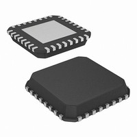
ISL54230IRTZ-T Intersil, ISL54230IRTZ-T Datasheet - Page 9

ISL54230IRTZ-T
Manufacturer Part Number
ISL54230IRTZ-T
Description
IC SWITCH QUAD DPDT 32TQFN
Manufacturer
Intersil
Datasheet
1.ISL54230IRTZ.pdf
(18 pages)
Specifications of ISL54230IRTZ-T
Function
Switch
Circuit
4 x DPDT
On-state Resistance
1.5 Ohm
Voltage Supply Source
Single Supply
Voltage - Supply, Single/dual (±)
2 V ~ 5.5 V
Current - Supply
1µA
Operating Temperature
-40°C ~ 85°C
Mounting Type
Surface Mount
Package / Case
32-WFQFN Exposed Pad
Lead Free Status / RoHS Status
Lead free / RoHS Compliant
Test Circuits and Waveforms
Detailed Description
The ISL54230 is a multiprotocol switch containing eight
switches configured as a Quad DPDT. Each DPDT switch is
independently controlled by a logic pin. The ISL54230 has
four switches that are compliant in passing USB2.0 signals
and four switches with low r
analog or digital signals such as audio or UART. It is offered
in a 36 ball WLCSP or a 32 Ld 5mmx5mm TQFN package
for applications which require small package size such as
cellphones and PDAs.
The ISL54230 contains four switches capable of passing
USB2.0 Full-Speed and High-Speed signals with minimal
distortion, two 1Ω switches and two 6Ω switches for
analog/digital signals. The USB capable switches were
designed with low capacitance and high bandwidth to pass
USB HS signals (480Mbps) with minimal edge and phase
distortion. The 1Ω switches are designed for passing low
bandwidth signals (<8MHz) and are ideal for switching
power lines since the low ON-resistance minimizes power
dissipation. The 6Ω switches are designed to pass audio or
data signals up to 100MHz while maintaining a low r
good THD performance.
In addition to the four independent logic control pins that
control each DPDT switch, the ISL54230 contains two Output
Enable (OE) logic pins that permits the IC to disable certain
switches giving the user a high degree of flexibility in signal
routing. Please see “OE Control Truth Table” on page 3 for an
explanation of the OE pins. All logic pins on the ISL54230 are
1.8V logic compatible up to a +3.3V supply.
OUT+
DIN+
DIN-
OUT-
FIGURE 6A. MEASUREMENT POINTS
90%
10%
90%
10%
t
t
t
fi
ri
f0
ON
t
50%
50%
ro
50%
9
50%
90%
that can be used to pass
10%
t
10%
90%
skew_i
t
skew_o
(Continued)
ON
FIGURE 6. SKEW TEST
for
ISL54230
|tro - tri| Delay Due to Switch for Rising Input and Rising Output Signals.
Power Supply Considerations
The power supply connected to the V
provides the DC bias voltage necessary to operate the IC.
The ISL54230 can be operated with a supply voltage in the
range of +2.0V to +5.5V. For USB applications, the supply
voltage should be in the range of +3.0V to +5.5V to ensure
proper signal levels on the USB data lines.
A decoupling capacitor in the range 0.01µF to 0.1µF should
be connected to the V
power supply noise that may be present on the supply lines.
The capacitor should be place as closed as possible to the
V
Supply Sequencing and Power-On Reset Protection
Proper power supply sequencing is necessary to protect the
ISL54230 from operating in fault conditions. The ISL54230
integrates Power-On Reset (POR) circuitry that prevents the
switches from turning ON until the supply voltage is at least
+1.4V. The POR has a 100mV hysteresis built in that will turn
the switches OFF when the supply has gone below +1.3V.
This function prevents signals from the switch input being
passed to the output when the device operating voltage has
not reached appropriate levels yet, protecting the switch
from fault conditions.
The POR circuitry also protects the switch from operating in
a fault condition should the power supply to the IC drop
below the POR threshold. Thus, the recommended
operational supply voltage is within +2.0V to +5.5V.
Operating at supply voltages below +2.0V may still be
functional but the noise margin between the POR threshold
and supply voltage will be reduced. The device may
|tfo - tfi| Delay Due to Switch for Falling Input and Falling Output Signals
|tskew_0| Change in Skew through the Switch for Output Signals.
|tskew_i| Change in Skew through the Switch for Input Signals.
DD
DIN+
DIN-
pin.
V
INx
15.8Ω
15.8Ω
143Ω
143Ω
FIGURE 6B. TEST CIRCUIT
INx
DD
COM2B
COM2A
V
GND
supply pin of the IC to filter out any
DD
C
OR NC2B
OR NC2A
NO2B
NO2A
DD
and GND pins
C
C
L
L
May 28, 2009
OUT+
45Ω
OUT-
45Ω
FN6825.2


