PHN210 NXP Semiconductors, PHN210 Datasheet
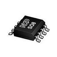
PHN210

Manufacturer Part Number
PHN210
Description
Manufacturer
NXP Semiconductors
Type
Power MOSFETr
Datasheet

Specifications of PHN210

Number Of Elements
2
Polarity
N
Channel Mode
Enhancement
Drain-source On-res
0.1Ohm
Drain-source On-volt
30V
Gate-source Voltage (max)
±20V
Continuous Drain Current
3.4A
Power Dissipation
2W
Operating Temp Range
-65C to 150C
Operating Temperature Classification
Military
Mounting
Surface Mount
Pin Count
8
Package Type
SO
Lead Free Status / Rohs Status
Compliant

Available stocks

Company
Part Number
Manufacturer
Quantity
Price
Part Number:
PHN210
Manufacturer:
NXP
Quantity:
30 000
Part Number:
PHN210
Manufacturer:
PHILIPS/飞利浦
Quantity:
20 000
Company:
Part Number:
PHN210
Quantity:
3 906
Part Number:
PHN210T
Manufacturer:
NXP
Quantity:
72 000
Part Number:
PHN210T
Manufacturer:
PHILIPS/飞利浦
Quantity:
20 000
Part Number:
PHN210TЈ¬118
Manufacturer:
NXP
Quantity:
7 500
Philips Semiconductors
FEATURES
• Dual device
• Low threshold voltage
• Fast switching
• Logic level compatible
• Surface mount package
GENERAL DESCRIPTION
Dual
mode field-effect transistor in a
plastic envelope using ’trench’
technology.
Applications:-
• Motor and relay drivers
• d.c. to d.c. converters
• Logic level translator
The PHN210 is supplied in the
SOT96-1 (SO8) surface mounting
package.
LIMITING VALUES
Limiting values in accordance with the Absolute Maximum System (IEC 134)
1 Surface mounted on FR4 board, t
January 2002
Dual N-channel enhancement mode
TrenchMOS
SYMBOL
V
V
V
V
I
I
I
P
T
D
D
DM
stg
DS
DS
DGR
GS
tot
, T
j
N-channel
PARAMETER
Repetitive peak drain-source
voltage
Continuous drain-source voltage
Drain-gate voltage
Gate-source voltage
Drain current per MOSFET
Drain current per MOSFET (both
MOSFETs conducting)
Drain current per MOSFET (pulse
peak value)
Total power dissipation (either or
both MOSFETs conducting)
Storage & operating temperature
TM
enhancement
transistor
1
10 sec
PINNING
SYMBOL
1
PIN
5,6
7,8
1
1
2
3
4
source 1
gate 1
source 2
gate 2
drain 2
drain 1
d1
s1
CONDITIONS
T
R
T
T
T
T
T
T
T
j
a
a
a
a
a
a
a
GS
= 25 ˚C to 150˚C
DESCRIPTION
= 25 ˚C
= 70 ˚C
= 25 ˚C
= 70 ˚C
= 25 ˚C
= 25 ˚C
= 70 ˚C
d1
g1
= 20 k
1
d2
s2
d2
g2
SOT96-1
QUICK REFERENCE DATA
R
R
DS(ON)
MIN.
DS(ON)
- 65
-
-
-
-
-
-
-
-
-
-
-
pin 1 index
200 m (V
100 m (V
V
I
Product specification
D
DS
= 3.4 A
MAX.
8
1
= 30 V
150
3.4
2.8
2.4
1.9
1.3
30
30
30
14
2
20
7
2
6
3
GS
GS
PHN210
= 4.5 V)
5
4
= 10 V)
Rev 1.100
UNIT
˚C
W
W
V
V
V
V
A
A
A
A
A

Related parts for PHN210

PHN210 Summary of contents

Page 1

... Applications:- • Motor and relay drivers • d.c. to d.c. converters • Logic level translator The PHN210 is supplied in the SOT96-1 (SO8) surface mounting package. LIMITING VALUES Limiting values in accordance with the Absolute Maximum System (IEC 134) SYMBOL ...

Page 2

... 2 Resistive load Measured from drain lead to centre of die Measured from source lead to source bond pad MHz Product specification PHN210 TYP. MAX. UNIT 10 sec - 62.5 150 - MIN. MAX. UNIT - 13 - 3.4 MIN. TYP. MAX. UNIT -55˚ 2.8 = 150˚C 0 -55˚C - 3.2 ...

Page 3

... Fig.3. Safe operating area ˚ f single pulse; parameter Zth j-a (K/ 0.5 0.2 0.1 0.05 0. single pulse 1E-05 1E-04 1E-03 1E-02 1E-01 Pulse width, tp (s) Fig.4. Transient thermal impedance f(t); parameter j-a p PHN210 2 1 PHN210 100 100 100 p PHN210 D = tp/T T 1E+00 1E+01 /T Rev 1.100 ...

Page 4

... Product specification Transconductance, gfs ( 150 Drain current parameter SOT223 30V Trench Normalised RDS(ON) = f(Tj 100 f(T DS(ON) DS(ON)25 ˚C VGS(TO max. typ. 2 min -60 -40 - 100 120 140 Fig.10. Gate threshold voltage. = f(T ); conditions mA; V GS(TO PHN210 ˚ 150 ) Rev 1.100 ...

Page 5

... Fig.14. Typical reverse diode current. = f(V ); conditions parameter T SDS GS Non-repetitive Avalanche current, IAS (A) Tj prior to avalanche =125 C VDS tp ID 1E-05 1E-04 1E-03 Avalanche time, tp (s) Fig.15. Maximum permissible non-repetitive ) versus avalanche time (t AS unclamped inductive load PHN210 j PHN210 25 C 1E- Rev 1.100 ...

Page 6

... REFERENCES IEC JEDEC EIAJ 076E03S MS-012AA Fig.16. SOT96 surface mounting package. 6 Product specification SOT96 detail X ( 1.0 0.7 0.7 0.25 0.25 0.1 0.4 0.6 0 0.039 0.028 0.028 0.01 0.01 0.004 0.016 0.024 0.012 EUROPEAN ISSUE DATE PROJECTION 95-02-04 97-05-22 PHN210 Rev 1.100 ...

Page 7

... This data sheet contains data from the product specification. Philips Semiconductors reserves the right to make changes at any time in order to improve the design, manufacturing and supply. Changes will be communicated according to the Customer Product/Process Change Notification (CPCN) procedure SNW-SQ-650A 7 Product specification PHN210 Rev 1.100 ...

Related keywords