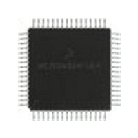
MC68HC711E9FU Freescale Semiconductor, MC68HC711E9FU Datasheet - Page 120

MC68HC711E9FU
Manufacturer Part Number
MC68HC711E9FU
Description
Manufacturer
Freescale Semiconductor
Datasheet
1.MC68HC711E9FU.pdf
(242 pages)
Specifications of MC68HC711E9FU
Cpu Family
HC11
Device Core Size
8b
Frequency (max)
4MHz
Interface Type
SCI/SPI
Program Memory Type
EPROM
Program Memory Size
12KB
Total Internal Ram Size
512Byte
# I/os (max)
38
Number Of Timers - General Purpose
8
Operating Supply Voltage (typ)
3.3/5V
Operating Supply Voltage (max)
5.5V
Operating Supply Voltage (min)
3V
On-chip Adc
8-chx8-bit
Instruction Set Architecture
CISC
Operating Temp Range
0C to 70C
Operating Temperature Classification
Commercial
Mounting
Surface Mount
Pin Count
64
Package Type
PQFP
Lead Free Status / Rohs Status
Not Compliant
Available stocks
Company
Part Number
Manufacturer
Quantity
Price
- Current page: 120 of 242
- Download datasheet (2Mb)
8.4 Clock Phase and Polarity Controls
Software can select one of four combinations of serial clock phase and polarity using two bits in the SPI
control register (SPCR). The clock polarity is specified by the CPOL control bit, which selects an active
high or active low clock, and has no significant effect on the transfer format. The clock phase (CPHA)
control bit selects one of two different transfer formats. The clock phase and polarity should be identical
for the master SPI device and the communicating slave device. In some cases, the phase and polarity
are changed between transfers to allow a master device to communicate with peripheral slaves having
different requirements.
When CPHA equals 0, the SS line must be negated and reasserted between each successive serial byte.
Also, if the slave writes data to the SPI data register (SPDR) while SS is low, a write collision error results.
When CPHA equals 1, the SS line can remain low between successive transfers.
120
Serial Peripheral Interface (SPI)
÷2 ÷4 ÷16 ÷32
MCU CLOCK
INTERNAL
SELECT
DIVIDER
SPI STATUS REGISTER
SPI CONTROL
SPI INTERRUPT
REQUEST
M68HC11E Family Data Sheet, Rev. 5.1
Figure 8-1. SPI Block Diagram
MSB
8--BIT SHIFT REGISTER
INTERNAL
DATA BUS
MSTR
SPE
READ DATA BUFFER
SPI CONTROL REGISTER
CLOCK
LOGIC
LSB
CLOCK
S
M
M
S
S
M
Freescale Semiconductor
MISO
MOSI
PD2
PD3
SCK
PD4
PD5
SS
Related parts for MC68HC711E9FU
Image
Part Number
Description
Manufacturer
Datasheet
Request
R

Part Number:
Description:
APPENDIX A ELECTRICAL CHARACTERISTICS
Manufacturer:
FREESCALE [Freescale Semiconductor, Inc]
Datasheet:
Part Number:
Description:
Manufacturer:
Freescale Semiconductor, Inc
Datasheet:
Part Number:
Description:
Manufacturer:
Freescale Semiconductor, Inc
Datasheet:
Part Number:
Description:
Manufacturer:
Freescale Semiconductor, Inc
Datasheet:
Part Number:
Description:
Manufacturer:
Freescale Semiconductor, Inc
Datasheet:
Part Number:
Description:
Manufacturer:
Freescale Semiconductor, Inc
Datasheet:
Part Number:
Description:
Manufacturer:
Freescale Semiconductor, Inc
Datasheet:
Part Number:
Description:
Manufacturer:
Freescale Semiconductor, Inc
Datasheet:
Part Number:
Description:
Manufacturer:
Freescale Semiconductor, Inc
Datasheet:
Part Number:
Description:
Manufacturer:
Freescale Semiconductor, Inc
Datasheet:
Part Number:
Description:
Manufacturer:
Freescale Semiconductor, Inc
Datasheet:
Part Number:
Description:
Manufacturer:
Freescale Semiconductor, Inc
Datasheet:
Part Number:
Description:
Manufacturer:
Freescale Semiconductor, Inc
Datasheet:
Part Number:
Description:
Manufacturer:
Freescale Semiconductor, Inc
Datasheet:
Part Number:
Description:
Manufacturer:
Freescale Semiconductor, Inc
Datasheet:


