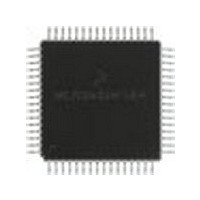
MC68HC711E9FU Freescale Semiconductor, MC68HC711E9FU Datasheet - Page 129

MC68HC711E9FU
Manufacturer Part Number
MC68HC711E9FU
Description
Manufacturer
Freescale Semiconductor
Datasheet
1.MC68HC711E9FU.pdf
(242 pages)
Specifications of MC68HC711E9FU
Cpu Family
HC11
Device Core Size
8b
Frequency (max)
4MHz
Interface Type
SCI/SPI
Program Memory Type
EPROM
Program Memory Size
12KB
Total Internal Ram Size
512Byte
# I/os (max)
38
Number Of Timers - General Purpose
8
Operating Supply Voltage (typ)
3.3/5V
Operating Supply Voltage (max)
5.5V
Operating Supply Voltage (min)
3V
On-chip Adc
8-chx8-bit
Instruction Set Architecture
CISC
Operating Temp Range
0C to 70C
Operating Temperature Classification
Commercial
Mounting
Surface Mount
Pin Count
64
Package Type
PQFP
Lead Free Status / Rohs Status
Not Compliant
Available stocks
Company
Part Number
Manufacturer
Quantity
Price
- Current page: 129 of 242
- Download datasheet (2Mb)
9.2 Timer Structure
Figure 9-2
for timer functions and for general-purpose I/O. For pins PA3, PA2, PA1, and PA0, this block contains
both the edge-detection logic and the control logic that enables the selection of which edge triggers an
input capture. The digital level on PA[3:0] can be read at any time (read PORTA register), even if the pin
is being used for the input capture function. Pins PA[6:3] are used for either general-purpose I/O, or as
output compare pins. When one of these pins is being used for an output compare function, it cannot be
written directly as if it were a general-purpose output. Each of the output compare functions (OC[5:2]) is
related to one of the port A output pins. Output compare one (OC1) has extra control logic, allowing it
optional control of any combination of the PA[7:3] pins. The PA7 pin can be used as a general-purpose
I/O pin, as an input to the pulse accumulator, or as an OC1 output pin.
9.3 Input Capture
The input capture function records the time an external event occurs by latching the value of the
free-running counter when a selected edge is detected at the associated timer input pin. Software can
store latched values and use them to compute the periodicity and duration of events. For example, by
storing the times of successive edges of an incoming signal, software can determine the period and pulse
width of a signal. To measure period, two successive edges of the same polarity are captured. To
measure pulse width, two alternate polarity edges are captured.
In most cases, input capture edges are asynchronous to the internal timer counter, which is clocked
relative to an internal clock (PH2). These asynchronous capture requests are synchronized to PH2 so that
the latching occurs on the opposite half cycle of PH2 from when the timer counter is being incremented.
This synchronization process introduces a delay from when the edge occurs to when the counter value is
detected. Because these delays offset each other when the time between two edges is being measured,
the delay can be ignored. When an input capture is being used with an output compare, there is a similar
delay between the actual compare point and when the output pin changes state.
Freescale Semiconductor
shows the capture/compare system block diagram. The port A pin control block includes logic
Control Bits
overflow —
overflow —
overflow —
overflow —
1 count —
1 count —
1 count —
1 count —
PR1, PR0
0 0
0 1
1 0
1 1
65.536 ms
262.14 ms
524.29 ms
4.0 MHz
1.0 MHz
1000 ns
1000 ns
16.0 µs
1.049 s
4.0 µs
8.0 µs
M68HC11E Family Data Sheet, Rev. 5.1
Table 9-1. Timer Summary
32.768 ms
131.07 ms
262.14 ms
524.29 ms
8.0 MHz
2.0 MHz
500 ns
500 ns
2.0 µs
4.0 µs
8.0 µs
Main Timer Count Rates
XTAL Frequencies
21.845 ms
87.381 ms
174.76 ms
349.52 ms
12.0 MHz
1.333 µs
2.667 µs
5.333 µs
3.0 MHz
333 ns
333 ns
Other Rates
(E/2
(E/2
(E/2
(E/2
(E/16)
(1/E)
(E/1)
(E/4)
(E/8)
(E)
16
18
19
20
)
)
)
)
Timer Structure
129
Related parts for MC68HC711E9FU
Image
Part Number
Description
Manufacturer
Datasheet
Request
R

Part Number:
Description:
APPENDIX A ELECTRICAL CHARACTERISTICS
Manufacturer:
FREESCALE [Freescale Semiconductor, Inc]
Datasheet:
Part Number:
Description:
Manufacturer:
Freescale Semiconductor, Inc
Datasheet:
Part Number:
Description:
Manufacturer:
Freescale Semiconductor, Inc
Datasheet:
Part Number:
Description:
Manufacturer:
Freescale Semiconductor, Inc
Datasheet:
Part Number:
Description:
Manufacturer:
Freescale Semiconductor, Inc
Datasheet:
Part Number:
Description:
Manufacturer:
Freescale Semiconductor, Inc
Datasheet:
Part Number:
Description:
Manufacturer:
Freescale Semiconductor, Inc
Datasheet:
Part Number:
Description:
Manufacturer:
Freescale Semiconductor, Inc
Datasheet:
Part Number:
Description:
Manufacturer:
Freescale Semiconductor, Inc
Datasheet:
Part Number:
Description:
Manufacturer:
Freescale Semiconductor, Inc
Datasheet:
Part Number:
Description:
Manufacturer:
Freescale Semiconductor, Inc
Datasheet:
Part Number:
Description:
Manufacturer:
Freescale Semiconductor, Inc
Datasheet:
Part Number:
Description:
Manufacturer:
Freescale Semiconductor, Inc
Datasheet:
Part Number:
Description:
Manufacturer:
Freescale Semiconductor, Inc
Datasheet:
Part Number:
Description:
Manufacturer:
Freescale Semiconductor, Inc
Datasheet:


