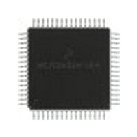
MC68HC711E9FU Freescale Semiconductor, MC68HC711E9FU Datasheet - Page 167

MC68HC711E9FU
Manufacturer Part Number
MC68HC711E9FU
Description
Manufacturer
Freescale Semiconductor
Datasheet
1.MC68HC711E9FU.pdf
(242 pages)
Specifications of MC68HC711E9FU
Cpu Family
HC11
Device Core Size
8b
Frequency (max)
4MHz
Interface Type
SCI/SPI
Program Memory Type
EPROM
Program Memory Size
12KB
Total Internal Ram Size
512Byte
# I/os (max)
38
Number Of Timers - General Purpose
8
Operating Supply Voltage (typ)
3.3/5V
Operating Supply Voltage (max)
5.5V
Operating Supply Voltage (min)
3V
On-chip Adc
8-chx8-bit
Instruction Set Architecture
CISC
Operating Temp Range
0C to 70C
Operating Temperature Classification
Commercial
Mounting
Surface Mount
Pin Count
64
Package Type
PQFP
Lead Free Status / Rohs Status
Not Compliant
Available stocks
Company
Part Number
Manufacturer
Quantity
Price
- Current page: 167 of 242
- Download datasheet (2Mb)
10.14 MC68L11E9/E20 Analog-to-Digital Converter Characteristics
Freescale Semiconductor
Resolution
Non-linearity
Zero error
Full scale error
Total unadjusted
Quantization error
Absolute accuracy
Conversion range
V
V
∆V
Conversion time
Monotonicity
Zero input reading
Full scale reading
Sample acquisition
Sample/hold
Input leakage
1. V
2. Source impedances greater than 10 kΩ affect accuracy adversely because of input leakage.
RH
RL
Characteristic
error
R
time
capacitance
DD
= 3.0 Vdc to 5.5 Vdc, V
(1)
Number of bits resolved by A/D converter
Maximum deviation from the ideal A/D transfer
Difference between the output of an ideal and an
Difference between the output of an ideal and an
Maximum sum of non-linearity, zero error, and
Uncertainty because of converter resolution
Difference between the actual input voltage and
Analog input voltage range
Maximum analog reference voltage
Minimum analog reference voltage
Minimum difference between V
Total time to perform a single
Conversion result never decreases with an
Conversion result when V
Conversion result when V
Analog input acquisition sampling time:
Input capacitance during sample
Input leakage on A/D pins
characteristics
actual for 0 input voltage
actual A/D for full-scale input voltage
full-scale error
the full-scale weighted equivalent of the binary
output code, all error sources included
analog-to-digital conversion:
increase in input voltage and has no missing
codes
E clock
Internal RC oscillator
PE[7:0]
PE[7:0]
V
RL
E clock
Internal RC oscillator
, V
SS
RH
= 0 Vdc, T
Parameter
M68HC11E Family Data Sheet, Rev. 5.1
A
= T
In
In
L
= V
= V
to T
(2)
RH
RL
RH
H,
and V
750 kHz ≤ E ≤ 2.0 MHz, unless otherwise noted
MC68L11E9/E20 Analog-to-Digital Converter Characteristics
RL
V
SS
Min
V
V
3.0
00
—
—
—
—
—
—
—
—
—
—
—
—
—
—
—
—
RL
RL
–0.1
Guaranteed
Absolute
20 typical
32
12
—
—
—
—
—
—
—
—
—
—
—
—
—
—
—
—
8
V
t
CYC
DD
Max
±1/2
±1/2
V
V
400
1.0
FF
±1
±1
±1
±2
12
—
—
—
—
—
—
—
RH
RH
+ 0.1
+ 32
Unit
t
t
LSB
LSB
LSB
LSB
LSB
LSB
Bits
Hex
Hex
CYC
CYC
pF
nA
µA
µs
—
µs
V
V
V
V
167
Related parts for MC68HC711E9FU
Image
Part Number
Description
Manufacturer
Datasheet
Request
R

Part Number:
Description:
APPENDIX A ELECTRICAL CHARACTERISTICS
Manufacturer:
FREESCALE [Freescale Semiconductor, Inc]
Datasheet:
Part Number:
Description:
Manufacturer:
Freescale Semiconductor, Inc
Datasheet:
Part Number:
Description:
Manufacturer:
Freescale Semiconductor, Inc
Datasheet:
Part Number:
Description:
Manufacturer:
Freescale Semiconductor, Inc
Datasheet:
Part Number:
Description:
Manufacturer:
Freescale Semiconductor, Inc
Datasheet:
Part Number:
Description:
Manufacturer:
Freescale Semiconductor, Inc
Datasheet:
Part Number:
Description:
Manufacturer:
Freescale Semiconductor, Inc
Datasheet:
Part Number:
Description:
Manufacturer:
Freescale Semiconductor, Inc
Datasheet:
Part Number:
Description:
Manufacturer:
Freescale Semiconductor, Inc
Datasheet:
Part Number:
Description:
Manufacturer:
Freescale Semiconductor, Inc
Datasheet:
Part Number:
Description:
Manufacturer:
Freescale Semiconductor, Inc
Datasheet:
Part Number:
Description:
Manufacturer:
Freescale Semiconductor, Inc
Datasheet:
Part Number:
Description:
Manufacturer:
Freescale Semiconductor, Inc
Datasheet:
Part Number:
Description:
Manufacturer:
Freescale Semiconductor, Inc
Datasheet:
Part Number:
Description:
Manufacturer:
Freescale Semiconductor, Inc
Datasheet:


