LF156H National Semiconductor, LF156H Datasheet - Page 4
LF156H
Manufacturer Part Number
LF156H
Description
Op Amps
Manufacturer
National Semiconductor
Type
General Purpose Amplifierr
Datasheet
1.LF156H.pdf
(23 pages)
Specifications of LF156H
Rail/rail I/o Type
No
Number Of Elements
1
Unity Gain Bandwidth Product
5MHz
Slew Rate
12V/us
Common Mode Rejection Ratio
85dB
Input Offset Voltage
5mV
Input Bias Current
100pA
Single Supply Voltage (typ)
Not RequiredV
Power Dissipation
1.2W
Voltage Gain In Db
106.02dB
Power Supply Rejection Ratio
85dB
Power Supply Requirement
Dual
Shut Down Feature
No
Single Supply Voltage (min)
Not RequiredV
Single Supply Voltage (max)
Not RequiredV
Dual Supply Voltage (max)
±22V
Technology
BiFET
Operating Temp Range
-55C to 125C
Operating Temperature Classification
Military
Mounting
Through Hole
Pin Count
8
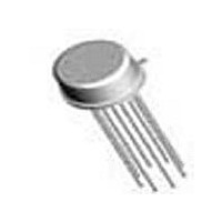
Package Type
TO-99
Number Of Channels
1
Voltage Gain Db
106.02 dB
Common Mode Rejection Ratio (min)
85 dB
Supply Current
7 mA at +/- 15 V
Maximum Power Dissipation
1200 mW
Maximum Operating Temperature
+ 125 C
Package / Case
TO-99
Maximum Dual Supply Voltage
+/- 22 V
Minimum Operating Temperature
- 55 C
Lead Free Status / Rohs Status
Not Compliant
Available stocks
Company
Part Number
Manufacturer
Quantity
Price

Part Number:
LF156H
Manufacturer:
NS/国半
Quantity:
20 000
Company:
Part Number:
LF156H/883C
Manufacturer:
NS
Quantity:
34
Company:
Part Number:
LF156H/883Q
Manufacturer:
NS
Quantity:
20
Company:
Part Number:
LF156H/NOPB
Manufacturer:
Microsemi
Quantity:
1 400


www.national.com
Notes for Electrical Characteristics
Supply Voltage, V
T
T
and V
Note 4: The Temperature Coefficient of the adjusted input offset voltage changes only a small amount (0.5µV/˚C typically) for each mV of adjustment from its original
unadjusted value. Common-mode rejection and open loop voltage gain are also unaffected by offset adjustment.
Note 5: The input bias currents are junction leakage currents which approximately double for every 10˚C increase in the junction temperature, T
production test time, the input bias currents measured are correlated to junction temperature. In normal operation the junction temperature rises above the ambient
temperature as a result of internal power dissipation, Pd. T
recommended if input bias current is to be kept to a minimum.
Note 6: Supply Voltage Rejection is measured for both supply magnitudes increasing or decreasing simultaneously, in accordance with common practice.
Note 7: Settling time is defined here, for a unity gain inverter connection using 2 k resistors for the LF155/6. It is the time required for the error voltage (the voltage
at the inverting input pin on the amplifier) to settle to within 0.01% of its final value from the time a 10V step input is applied to the inverter. For the LF357, A
the feedback resistor from output to input is 2k
Note 8: Max. Power Dissipation is defined by the package characteristics. Operating the part near the Max. Power Dissipation may cause the part to operate outside
guaranteed limits.
Typical DC Performance Characteristics
specified.
A
HIGH
OS
, I
B
and I
OS
are measured at V
S
Input Bias Current
Input Bias Current
±
−55˚C
+125˚C
CM
15V
= 0.
LF155/156
V
and the output step is 10V (See Settling Time Test Circuit).
T
S
A
±
+125˚C
20V
00564639
00564637
J
= T
A
+
JA
−25˚C
+85˚C
±
Pd where
15V
(Continued)
LF256/257
4
V
T
S
JA
A
Curves are for LF155 and LF156 unless otherwise
is the thermal resistance from junction to ambient. Use of a heat sink is
±
+85˚C
20V
0˚C
+70˚C
±
15V
Input Bias Current
Voltage Swing
LF356B
T
A
V
S
+70˚C
±
20V
V
0˚C
+70˚C
S
=
00564638
00564640
LF355/6/7
±
J
T
. Due to limited
15V
A
+70˚C
V
= −5,
Related parts for LF156H
Image
Part Number
Description
Manufacturer
Datasheet
Request
R

Part Number:
Description:
National Semiconductor [8-Bit D/A Converter]
Manufacturer:
National Semiconductor
Datasheet:
Part Number:
Description:
National Semiconductor [Media Coprocessor]
Manufacturer:
National Semiconductor
Datasheet:
Part Number:
Description:
Digitally Controlled Tone and Volume Circuit with Stereo Audio Power Amplifier, Microphone Preamp Stage and National 3D Sound
Manufacturer:
National Semiconductor
Datasheet:
Part Number:
Description:
Digitally Controlled Tone and Volume Circuit with Stereo Audio Power Amplifier, Microphone Preamp Stage and National 3D Sound
Manufacturer:
National Semiconductor
Datasheet:
Part Number:
Description:
AC97 Rev 2 Codec with Sample Rate Conversion and National 3D Sound
Manufacturer:
National Semiconductor
Part Number:
Description:
Manufacturer:
National Semiconductor
Datasheet:
Part Number:
Description:
Manufacturer:
National Semiconductor
Datasheet:
Part Number:
Description:
General Purpose, Low Voltage, Low Power, Rail-to-Rail Output Operational Amplifiers
Manufacturer:
National Semiconductor
Datasheet:
Part Number:
Description:
8-bit 20 MSPS flash A/D converter.
Manufacturer:
National Semiconductor
Datasheet:
Part Number:
Description:
Low Noise Quad Operational Amplifier
Manufacturer:
National Semiconductor
Datasheet:
Part Number:
Description:
Quad Differential Line Receivers
Manufacturer:
National Semiconductor
Datasheet:
Part Number:
Description:
Quad High Speed Trapezoidal? Bus Transceiver
Manufacturer:
National Semiconductor
Datasheet:
Part Number:
Description:
Dual Line Receiver
Manufacturer:
National Semiconductor
Datasheet:
Part Number:
Description:
TTL to 10k ECL Level Translator with Latch
Manufacturer:
National Semiconductor
Datasheet: