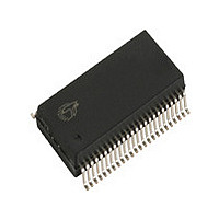
CY28159PVC Cypress Semiconductor Corp, CY28159PVC Datasheet

CY28159PVC
Specifications of CY28159PVC
Available stocks
Related parts for CY28159PVC
CY28159PVC Summary of contents
Page 1
... VCO SEL100/133 PD# S(0,1) Intel is a registered trademark of Intel Corporation. Cypress Semiconductor Corporation Document #: 38-07118 Rev. *A • All outputs compliant with Intel • External resistor for current reference • Selection logic for differential swing control, test mode, Hi-Z, power-down and spread spectrum • ...
Page 2
Pin Description Pin Name I/O 20 SSCG 7,10, 13, 16, CPU(0:7) 42, 39, 36 11, 14, 17, CPU(0:7)# 41, 38, 35 IRef 1 3V33 44 PD 48M(0,1), S(0,1) 48 SEL100/133 23 XOUT 22 XIN ...
Page 3
Table 2. Group Offset Specifications Group Offset CPU to 3V33 No requirement CPU to REF No requirement Test Load Configuration The following shows test load configurations for the different Host Clock Outputs.(MULTsel1 = 0, MULTsel0 =1 CPUT VDD MULTSEL CPUT# ...
Page 4
Document #: 38-07118 Rev ...
Page 5
Spread Spectrum Clock Generation (SSCG) Spread Spectrum is a modulation technique applied here for maximum efficiency in minimizing Electro-Magnetic Interfer- Table 4. Spectrum Spreading Selection Table Unspread Frequency in MHz 100 133.3 200 Power Management Functions Table 5. Host Swing ...
Page 6
Buffer Characteristics Current Mode CPU Clock Buffer Characteristics The current mode output buffer detail and current reference circuit details are contained elsewhere in this datasheet. The following parameters are used to specify output buffer charac- teristics: VDD3 (3.3V +/- 5%) ...
Page 7
Table 7. Current Accuracy Conditions Iout V = nominal (3.30V) All combinations of M0, M1 and Rr shown in DD Host Swing Select Function, Table 5 on page 5 Iout V = 3.30 ± 5% All combinations of M0, m1 ...
Page 8
Maximum Ratings Input Voltage Relative to V :...............................V SS Input Voltage Relative ............. V DDQ DD Storage Temperature: ................................ – 150 C Operating Temperature: .................................... +70 C Maximum ...
Page 9
AC Parameters ( 3.3V ±5 DDA Symbol Description TPeriod CPU(0:7), (0:7)#) Period Tr/Tf CPU[(0:7), (0:7)#] Rise and Fall Times TSKEW1 Skew from Any CPU Pair to Any CPU Pair TCJJ CPU[(0:7), (0:7)#] Cycle to Cycle ...
Page 10
Sample Layout +3.3V Supply Dale ILB1206 - 300 (300 @ 100 MHz) Cermaic Caps C1 & 10–22 µ VIA to GND plane layer Note: Each supply plane or strip should have a ...
Page 11
... Ordering Information Part Number CY28159PVC CY28159PVCT CY28159ZC CY28159ZCT Package Drawing and Dimensions 48-Lead Shrunk Small Outline Package O48 Document #: 38-07118 Rev. *A Package Type 48-Pin SSOP 48-Pin SSOP - Tape and Reel 48-Pin TSSOP 48-Pin TSSOP - Tape and Reel CY28159 Product Flow Commercial ...
Page 12
... Document #: 38-07118 Rev. *A © Cypress Semiconductor Corporation, 2002. The information contained herein is subject to change without notice. Cypress Semiconductor Corporation assumes no responsibility for the use of any circuitry other than circuitry embodied in a Cypress Semiconductor product. Nor does it convey or imply any license under patent or other rights. Cypress Semiconductor does not authorize its products for use as critical components in life-support systems where a malfunction or failure may reasonably be expected to result in significant injury to the user ...
Page 13
Document Title: CY28159 Clock Generator for Serverworks Grand Champion Chipset Applications Document Number: 38-07118 Issue Orig. of REV. ECN NO. Date Change ** 111426 01/22/02 *A 122789 12/27/02 Document #: 38-07118 Rev. *A Description of Change DMG New data sheet ...


