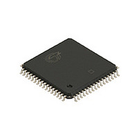
CY7C4265V-15ASI Cypress Semiconductor Corp, CY7C4265V-15ASI Datasheet - Page 12

CY7C4265V-15ASI
Manufacturer Part Number
CY7C4265V-15ASI
Description
Manufacturer
Cypress Semiconductor Corp
Datasheet
1.CY7C4265V-15ASI.pdf
(21 pages)
Specifications of CY7C4265V-15ASI
Configuration
Dual
Density
288Kb
Access Time (max)
15ns
Word Size
18b
Organization
16Kx18
Sync/async
Synchronous
Expandable
Yes
Bus Direction
Uni-Directional
Package Type
TQFP
Clock Freq (max)
66.7MHz
Operating Supply Voltage (typ)
3.3V
Operating Supply Voltage (min)
3V
Operating Supply Voltage (max)
3.6V
Supply Current
35mA
Operating Temp Range
-40C to 85C
Operating Temperature Classification
Industrial
Mounting
Surface Mount
Pin Count
64
Lead Free Status / Rohs Status
Not Compliant
Switching Waveforms
Notes
Document #: 38-06012 Rev. *B
19. The clocks (RCLK, WCLK) can be free-running during reset.
20. After reset, the outputs are LOW if OE = 0 and three-state if OE = 1.
21. When t
22. The first word is always available the cycle after EF goes HIGH.
t
SKEW2
Q
D
REN, WEN,
0
0
WCLK
RCLK
WEN
–D
–Q
REN
Q
EF,PAE
FF,PAF,
OE
. The Latency Timing applies only at the Empty Boundary (EF = LOW).
SKEW2
EF
0 –
17
17
RS
Q
HF
LD
17
> minimum specification, t
t
ENS
t
DS
Figure 9. First Data Word Latency after Reset with Simultaneous Read and Write
D
0
(FIRSTVALID WRITE)
(continued)
FRL
(maximum) = t
t
SKEW2
t
t
t
RSF
RSF
RSF
t
t
OLZ
RS
t
FRL
CLK
[21]
Figure 8. Reset Timing
+ t
SKEW2
t
D
REF
. When t
1
SKEW2
t
OE
< minimum specification, t
[19]
t
D
t
A
RSR
2
CY7C4255V, CY7C4265V
CY7C4275V, CY7C4285V
FRL
(maximum) = either 2*t
D
0
t
A
[22]
D
3
OE=0
OE=1
CLK
+ t
[20]
Page 12 of 21
SKEW2
D
1
D
or t
4
CLK
+
[+] Feedback


