AD8803AR-REEL Analog Devices Inc, AD8803AR-REEL Datasheet
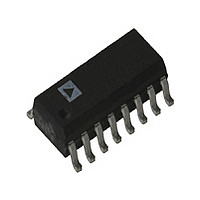
AD8803AR-REEL

Manufacturer Part Number
AD8803AR-REEL
Description
Manufacturer
Analog Devices Inc
Datasheet

Specifications of AD8803AR-REEL

Number Of Channels
8
Resolution
8b
Conversion Rate
1.7MSPS
Interface Type
Serial (3-Wire/SPI)
Single Supply Voltage (typ)
3/5V
Dual Supply Voltage (typ)
Not RequiredV
Settling Time
0.6us
Architecture
R-2R
Power Supply Requirement
Single
Output Type
Voltage
Integral Nonlinearity Error
±1.5LSB
Single Supply Voltage (min)
2.7V
Single Supply Voltage (max)
5.5V
Dual Supply Voltage (min)
Not RequiredV
Dual Supply Voltage (max)
Not RequiredV
Operating Temp Range
-40C to 85C
Operating Temperature Classification
Industrial
Mounting
Surface Mount
Pin Count
16
Package Type
SOIC N
Lead Free Status / Rohs Status
Not Compliant
a
GENERAL DESCRIPTION
The AD8801/AD8803 provides eight digitally controlled dc
voltage outputs. This potentiometer divider TrimDAC
replacement of the mechanical trimmer function in new designs.
The AD8801/AD8803 is ideal for dc voltage adjustment
applications.
Easily programmed by serial interfaced microcontroller ports,
the AD8801 with its midscale preset is ideal for potentiometer
replacement where adjustments start at a nominal value. Appli-
cations such as gain control of video amplifiers, voltage con-
trolled frequencies and bandwidths in video equipment,
geometric correction and automatic adjustment in CRT com-
puter graphic displays are a few of the many applications ideally
suited for these parts. The AD8803 provides independent con-
trol of both the top and bottom end of the potentiometer divider
allowing a separate zero-scale voltage setting determined by the
V
vices with a limited allowable voltage control range.
See the AD8802/AD8804 for a twelve channel version of this product.
TrimDAC is a registered trademark of Analog Devices, Inc.
REV. A
Information furnished by Analog Devices is believed to be accurate and
reliable. However, no responsibility is assumed by Analog Devices for its
use, nor for any infringements of patents or other rights of third parties
which may result from its use. No license is granted by implication or
otherwise under any patent or patent rights of Analog Devices.
REFL
FEATURES
Low Cost
Replaces Eight Potentiometers
Eight Individually Programmable Outputs
Three-Wire Serial Input
Power Shutdown
Midscale Preset, AD8801
Separate V
+3 V to +5 V Single Supply Operation
APPLICATIONS
Automatic Adjustment
Trimmer Potentiometer Replacement
Video and Audio Equipment Gain and Offset Adjustment
Portable and Battery Operated Equipment
pin. This is helpful for maximizing the resolution of de-
REFL
Range Setting, AD8803
25 W Including I
DD
and I
REF
®
allows
Internally the AD8801/AD8803 contain eight voltage output
digital-to-analog converters, sharing a common reference volt-
age input.
Each DAC has its own DAC register that holds its output state.
These DAC registers are updated from an internal serial-to-par-
allel shift register that is loaded from a standard three-wire serial
input digital interface. Eleven data bits make up the data word
clocked into the serial input register. This data word is decoded
where the first 3 bits determine the address of the DAC register
to be loaded with the last 8 bits of data. The AD8801/AD8803
consumes only 5 A from 5 V power supplies. In addition, in
shutdown mode reference input current consumption is also re-
duced to 5 A while saving the DAC latch settings for use after
return to normal operation.
The AD8801/AD8803 is available in 16-pin plastic DIP and the
1.5 mm height SO-16 surface mount packages.
One Technology Way, P.O. Box 9106, Norwood. MA 02062-9106, U.S.A.
Tel: 617/329-4700
GND
CLK
V
SDI
CS
DD
AD8801/AD8803
FUNCTIONAL BLOCK DIAGRAM
(DACs 2–7 Omitted for Clarity)
ADDRESS
SELECT
SERIAL
D
LATCH
CK RS
11-BIT
DAC
3
with Power Shutdown
1
8
8
Octal 8-Bit TrimDAC
AD8801/AD8803
RS
8
8
CK RS
LATCH
CK RS
LATCH
8-BIT
8-BIT
V
REFH
8
© Analog Devices, Inc., 1995
V
REFL
V
V
V
V
REFH
REFH
REFL
DAC 1 V
REFL
8
DAC 8 V
8
Fax: 617/326-8703
.
.
.
.
.
.
SHDN
OUT
OUT
O1
O8

Related parts for AD8803AR-REEL

AD8803AR-REEL Summary of contents

Page 1

FEATURES Low Cost Replaces Eight Potentiometers Eight Individually Programmable Outputs Three-Wire Serial Input Power Shutdown 25 W Including I Midscale Preset, AD8801 Separate V Range Setting, AD8803 REFL + Single Supply Operation APPLICATIONS Automatic Adjustment ...

Page 2

AD8801/AD8803–SPECIFICATIONS Parameter STATIC ACCURACY Specifications Apply to All DACs Resolution Integral Nonlinearity Error Differential Nonlinearity Full-Scale Error Zero-Code Error DAC Output Resistance Output Resistance Match REFERENCE INPUT 2 Voltage Range Input Resistance 3 Reference Input Capacitance DIGITAL INPUTS Logic High ...

Page 3

... Therefore, proper ESD precautions are recommended to avoid performance degradation or loss of functionality. REV. A Model FTN DD DD AD8801AN RS DD AD8801AR RS AD8803AN REFL AD8803AR REFL MAX – Pin Name Description 1 V Common High-Side DAC Reference Input REFH 2 ...

Page 4

AD8801/AD8803 OCTAL 8-BIT TRIMDAC, WITH SHUTDOWN 1 SDI CLK 0 1 DAC REGISTER LOAD CS 0 +5V V OUT 0V Figure 2a. Timing Diagram DETAIL SERIAL DATA ...

Page 5

For example, when and V REFH ing output voltages will be generated for the following codes Output State REFH 255 4.98 V Full-Scale 128 2.50 V Half-Scale (Midscale ...

Page 6

AD8801/AD8803–Typical Performance Characteristics + +5V 0.75 REFH REFL 0.5 0.25 0 –0.25 –0.5 –0.75 – 128 CODE – Decimal Figure 7. INL vs. Code ...

Page 7

V = +3V DD 0.001 0.0001 0 0.5 1 1.5 2 2.5 LOGIC INPUT VOLTAGE – Volts Figure 13. Supply Current vs. Logic Input Voltage +5V 0. ...

Page 8

AD8801/AD8803 0. 0. – 2 –0.02 –0.04 0 150 300 HOURS OF OPERATION AT 150 C Figure 19. Full-Scale Error Accelerated by Burn-In APPLICATIONS Supply Bypassing Precision analog products, such as the AD8801/AD8803, re- ...

Page 9

V V REFH DD OP291 100k AD8801/ AD8803 V GND REFL DIGITAL INTERFACING OMITTED FOR CLARITY Figure 23. Buffering the AD8801/AD8803 Output Increasing Output Voltage Swing ...

Page 10

AD8801/AD8803 ; ; This subroutine loads an AD8801/AD8803 DAC from an 8051 microcomputer, ; using the 8051’s serial port in MODE 0 (Shift Register Mode). ; The DAC value is stored at location DAC_VAL ; The DAC address is stored ...

Page 11

The subroutine begins by setting appropriate bits in the Serial Control register to configure the serial port for Mode 0 opera- tion. Next the DAC’s Chip Select input is set low to enable the AD8801/AD8803. The DAC address is obtained ...

Page 12

AD8801/AD8803 8051 µC P1.7 P1.6 P1.5 P1.4 PORT 1 1.7 1.6 1.5 1.4 Figure 26. An AD8801/AD8803-8051 C Interface Using Parallel Port 1 Unlike the serial port interface of Figure 25, the parallel port in- terface only transmits 11 bits ...

Page 13

AD8801/AD8803 to M68HC11 Interface Assembly Program * * M68HC11 Register definitions * PORTC EQU $1003 * DDRC EQU $1007 PORTD EQU $1008 * DDRD EQU $1009 SPCR EQU $1028 * SPSR EQU $1029 * SPDR EQU $102A * ...

Page 14

AD8801/AD8803 PSHY PSHA * * Enter Contents of SDI1 Data Register * LDAA $0000 STAA SDI1 * * Enter Contents of SDI2 Data Register * LDAA $0001 STAA SDI2 * LDX #SDI1 LDY #$1000 * * Reset AD8801 to one-half ...

Page 15

PIN 1 0.0098 (0.25) 0.0040 (0.10) REV. A OUTLINE DIMENSIONS Dimensions shown in inches and (mm). 16-Pin Plastic DIP Package (N-16) 0.840 (21.33) 0.745 (18.93 0.280 (7.11) 0.240 (6.10 0.325 ...

Page 16

–16– ...

Related keywords