MTB33N10E ON Semiconductor, MTB33N10E Datasheet - Page 7
MTB33N10E
Manufacturer Part Number
MTB33N10E
Description
Manufacturer
ON Semiconductor
Type
Power MOSFETr
Datasheet
1.MTB33N10E.pdf
(10 pages)
Specifications of MTB33N10E
Number Of Elements
1
Polarity
N
Channel Mode
Enhancement
Drain-source On-res
0.06Ohm
Drain-source On-volt
100V
Gate-source Voltage (max)
±20V
Continuous Drain Current
33A
Power Dissipation
2.5W
Operating Temp Range
-55C to 150C
Operating Temperature Classification
Military
Mounting
Surface Mount
Pin Count
2 +Tab
Package Type
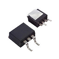
D2PAK
Dc
0106
Lead Free Status / Rohs Status
Not Compliant
Available stocks
Company
Part Number
Manufacturer
Quantity
Price
Company:

Part Number:
MTB33N10E
Manufacturer:
ON
Quantity:
1 537


total design. The footprint for the semiconductor packages
must be the correct size to ensure proper solder connection
function of the drain pad size. These can vary from the
minimum pad size for soldering to a pad size given for
maximum power dissipation. Power dissipation for a
surface mount device is determined by T
maximum rated junction temperature of the die, R
thermal resistance from the device junction to ambient, and
the operating temperature, T
on the data sheet, P
ratings table on the data sheet. Substituting these values
into the equation for an ambient temperature T
one can calculate the power dissipation of the device. For a
D
2
Surface mount board layout is a critical portion of the
The power dissipation for a surface mount device is a
The values for the equation are found in the maximum
PAK device, P
INFORMATION FOR USING THE D
P
D
RECOMMENDED FOOTPRINT FOR SURFACE MOUNTED APPLICATIONS
D
D
is calculated as follows.
=
can be calculated as follows:
T
J(max)
POWER DISSIPATION FOR A SURFACE MOUNT DEVICE
A
R
. Using the values provided
θJA
10.66
0.42
− T
°
70
60
50
40
30
20
A
0
Figure 16. Thermal Resistance versus Drain Pad
Area for the D
2
J(max)
A
0.33
8.38
2.5 Watts
of 25°C,
3.5 Watts
θJA
4
http://onsemi.com
, the
A, Area (square inches)
, the
5 Watts
17.02
0.63
6
Board Material = 0.0625″
G−10/FR−4, 2 oz Copper
2
PAK Package (Typical)
2
7
PAK SURFACE MOUNT PACKAGE
8
interface between the board and the package. With the
correct pad geometry, the packages will self align when
subjected to a solder reflow process.
the recommended footprint on a glass epoxy printed circuit
board to achieve a power dissipation of 2.5 Watts. There are
other alternatives to achieving higher power dissipation
from the surface mount packages. One is to increase the
area of the drain pad. By increasing the area of the drain
pad, the power dissipation can be increased. Although one
can almost double the power dissipation with this method,
one will be giving up area on the printed circuit board
which can defeat the purpose of using surface mount
technology. For example, a graph of R
area is shown in Figure 16.
The 50°C/W for the D
0.12
3.05
10
12
2.032
1.016
0.08
0.04
P
D
T
A
= 150°C − 25°C
14
= 25°C
6.096
inches
0.24
mm
50°C/W
16
2
PAK package assumes the use of
= 2.5 Watts
θJA
versus drain pad
Related parts for MTB33N10E
Image
Part Number
Description
Manufacturer
Datasheet
Request
R

Part Number:
Description:
ON Semiconductor [VOLTAGE REGULATOR]
Manufacturer:
ON Semiconductor
Datasheet:
Part Number:
Description:
357-036-542-201 CARDEDGE 36POS DL .156 BLK LOPRO
Manufacturer:
ON Semiconductor
Datasheet:
Part Number:
Description:
357-036-542-201 CARDEDGE 36POS DL .156 BLK LOPRO
Manufacturer:
ON Semiconductor
Datasheet:
Part Number:
Description:
357-036-542-201 CARDEDGE 36POS DL .156 BLK LOPRO
Manufacturer:
ON Semiconductor
Datasheet:
Part Number:
Description:
357-036-542-201 CARDEDGE 36POS DL .156 BLK LOPRO
Manufacturer:
ON Semiconductor
Datasheet:
Part Number:
Description:
357-036-542-201 CARDEDGE 36POS DL .156 BLK LOPRO
Manufacturer:
ON Semiconductor
Datasheet:
Part Number:
Description:
357-036-542-201 CARDEDGE 36POS DL .156 BLK LOPRO
Manufacturer:
ON Semiconductor
Datasheet:
Part Number:
Description:
357-036-542-201 CARDEDGE 36POS DL .156 BLK LOPRO
Manufacturer:
ON Semiconductor
Datasheet:
Part Number:
Description:
357-036-542-201 CARDEDGE 36POS DL .156 BLK LOPRO
Manufacturer:
ON Semiconductor
Datasheet:
Part Number:
Description:
357-036-542-201 CARDEDGE 36POS DL .156 BLK LOPRO
Manufacturer:
ON Semiconductor
Datasheet:
Part Number:
Description:
357-036-542-201 CARDEDGE 36POS DL .156 BLK LOPRO
Manufacturer:
ON Semiconductor
Datasheet:
Part Number:
Description:
Manufacturer:
ON Semiconductor
Datasheet:
Part Number:
Description:
Manufacturer:
ON Semiconductor
Datasheet:
Part Number:
Description:
Manufacturer:
ON Semiconductor
Datasheet: