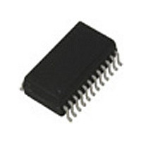
L9823 STMicroelectronics, L9823 Datasheet

L9823
Specifications of L9823
Available stocks
Related parts for L9823
L9823 Summary of contents
Page 1
... OUTPUT MODE PROGRAMMABLE FOR SUSTAINED CURRENT LIMIT OR SHUTDOWN DESCRIPTION L9823 is a Octal Low-Side Driver Circuit, dedicated for automotive applications. Output voltage clamping is provided for flyback current recirculation, when in- ductive loads are driven. Chip Select and cascadable Serial 8-bit Interface for outputs control and diagnos- tic data transfer ...
Page 2
... CSB. The system MCU selects the L9823 to be communicated with through the use of the CSB pin. Whenever the pin logic low state, data can be transferred from the MCU to the L9823 and vise versa. Clocked-in data from the MCU is transferred from the L9823 shift register and latched into the power outputs on the rising edge of the CSB signal ...
Page 3
... MCU open circuit. The internal pull- afford safe and easy interfacing to the MCU. The Reset pin of the L9823 should be pulled to a logic low state for a duration of at least 160ns to ensure reliable Reset. ...
Page 4
... L9823 ABSOLUTE MAXIMUM RATINGS (continued) Symbol V Continuous output current OUT Cont I Output current OUT PEAK E Output clamp energy OUTclamp I Output current (self limit) OUT LIM Note 1) All inputs are protected against ESD according to MIL 883C; tested with HBM C = 100pF 1500 a dissipated energy E ...
Page 5
... OUT DG SFPD = Low OUT DG CSB = 50 1/2 I OUT OUT LIM out DG Output programmed OFF SFPD = Low OUT DG CSB = 50% to valid data at SO CSB = 50 0, 16V OUT bat bat L9823 Min. Typ. Max. Unit -10 10 µA 50 250 -0 0.4 V -10 10 µ -10 10 µA < 1.5 ...
Page 6
... L9823 ELECTRICAL CHARACTERISTCS (continued) Symbol Parameter t Turn OFF delay doff dV Turn ON voltage slew-rate on/dt dV Turn OFF voltage slew-rate off/dt dV Turn OFF voltage clamp slew-rate 30 off clamp/dt Serial diagnostic link (Load capacitor 200pF) f Clock frequency sclk t Minimum time SCLK = HIGH clh ...
Page 7
... For the load diagnostic in output off condition each output features a diagnostic current sink, of typ 60µA. FUNCTIONAL DESCRIPTION General The L9823 integrated circuit features 8 power low-side-driver outputs. Data is transmitted to the device using the Serial Peripheral Interface = SPI protocol. The power outputs features voltage clamping function for flyback current recirculation and are protected against short circuit to Vbat. ...
Page 8
... L9823 Output Stages Control Each output is controlled with its latch and with a common Reset line, which enables all outputs. The control data are transmitted via the SI input, the timing of the serial interface is shown in Fig. 1. The device is selected with low CSB signal and the input data are transferred into the 8 bit shift register at every falling SCLK edge ...
Page 9
... Figure 2. Pulse Diagram to Read the Outputs Status Register CSB SCLK SI SO Figure 3. Structure of the Outputs Status Register MSB Diag7 Diag6 Diag5 MSB MSB LSB Diag4 Diag3 Diag2 Diag1 Diag0 2 1 LSB 2 1 LSB Diagnostic-bit ou Diagnostic-bit ou Diagnostic-bit ou Diagnostic-bit ou Diagnostic-bit ou Diagnostic-bit ou Diagnostic-bit ou Diagnostic-bit ou L9823 9/12 ...
Page 10
... L9823 APPLICATIONS INFORMATION The typical application diagram for parallel Input SPI control is shown in Figure 4. Figure 4. Typical Application Circuit Diagram for the L9823 Circuit. SFPD 15 CSB 10 SCLK Reset 22 µP Undervoltage For higher current driving capability more outputs of the same kind can be paralleled. In this case the maximum flyback energy should not exceed the limit value for single output ...
Page 11
... Mold flash, protusions or gate burrs shall not exceed 0.15mm per side. inch TYP. MAX. MECHANICAL DATA 0.104 0.012 0.200 Weight: 0.60gr 0.013 0.614 0.299 0.050 0.419 0.030 0.050 0.004 L9823 OUTLINE AND SO24 0070769 C 11/12 ...
Page 12
... L9823 Information furnished is believed to be accurate and reliable. However, STMicroelectronics assumes no responsibility for the consequences of use of such information nor for any infringement of patents or other rights of third parties which may result from its use. No license is granted by implication or otherwise under any patent or patent rights of STMicroelectronics. Specifications mentioned in this publication are subject to change without notice ...


