STV0299B STMicroelectronics, STV0299B Datasheet
STV0299B
Specifications of STV0299B
Available stocks


Related parts for STV0299B


STV0299B Summary of contents
Page 1
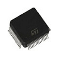
... Its low power consumption, small package and optional serial output interface makes it perfect for embedding into a tuner. STV0299B QPSK/BPSK LINK IC TQFP64 ( 1.4 mm) (Thin Plastic Quad Flat Pack) ORDER CODE: STV0299B (No Slug) SATELLITE RECEIVER specifications. Processing is fully digital. sampling rate facilitates 2 C ...
Page 2
... STV0299B TABLE OF CONTENTS 1 PIN INFORMATION . . . . . . . . . . . . . . . . . . . . . . . . . . . . . . . . . . . . . . . . . . . . . . . . . . . . . . . . . . . . . . 4 1.1 Pin Connections . . . . . . . . . . . . . . . . . . . . . . . . . . . . . . . . . . . . . . . . . . . . . . . . . . . . . . . . . . . 4 1.2 Pinout Description BLOCK DIAGRAM . . . . . . . . . . . . . . . . . . . . . . . . . . . . . . . . . . . . . . . . . . . . . . . . . . . . . . . . . . . . . . . 6 3 SYSTEM CHARACTERISTICS . . . . . . . . . . . . . . . . . . . . . . . . . . . . . . . . . . . . . . . . . . . . . . . . . . . . . 6 4 FUNCTIONAL DESCRIPTION . . . . . . . . . . . . . . . . . . . . . . . . . . . . . . . . . . . . . . . . . . . . . . . . . . . . . . 7 4.1 Front End Interfaces . . . . . . . . . . . . . . . . . . . . . . . . . . . . . . . . . . . . . . . . . . . . . . . . . . . . . . . . 7 2 4.1 Interface . . . . . . . . . . . . . . . . . . . . . . . . . . . . . . . . . . . . . . . . . . . . . . . . . . . . . . . . . . . 7 4.1.2 Write Operation (Normal Mode 4.1.3 Read Operation (Normal Mode 4.1 Interface in Standby Mode . . . . . . . . . . . . . . . . . . . . . . . . . . . . . . . . . . . . . . . . . . . . . 7 4.1.5 Specific Concerns about SCL Frequency . . . . . . . . . . . . . . . . . . . . . . . . . . . . . . . . . . . . 8 4 ...
Page 3
... TABLE OF CONTENTS (continued) 6.2 Thermal Data . . . . . . . . . . . . . . . . . . . . . . . . . . . . . . . . . . . . . . . . . . . . . . . . . . . . . . . . . . . . . 29 6.3 DC Electrical Characteristics . . . . . . . . . . . . . . . . . . . . . . . . . . . . . . . . . . . . . . . . . . . . . . . . 29 6.4 Timing Characteristics . . . . . . . . . . . . . . . . . . . . . . . . . . . . . . . . . . . . . . . . . . . . . . . . . . . . . Bus Characteristics APPLICATION BLOCK DIAGRAMS . . . . . . . . . . . . . . . . . . . . . . . . . . . . . . . . . . . . . . . . . . . . . . . . 33 8 PACKAGE MECHANICAL DATA . . . . . . . . . . . . . . . . . . . . . . . . . . . . . . . . . . . . . . . . . . . . . . . . . . 35 STV0299B Page 3/36 ...
Page 4
... STV0299B 1 PIN INFORMATION 1.1 Pin Connections Figure 1: Pinout for 64-pin TQFP (10x10 mm CLK_IN/XTAL_IN 1 XTAL_OUT 2 V SSA 3 V DDA 4 AUX_CLK AGC SDA 12 V DD_3 SCL 14 RESET 15 F22/DiSEqC 4/ TEST 46 TEST 45 TEST 44 TEST 43 STDBY DAC IP0 38 TEST BOT DDA DD SS ...
Page 5
... ADC Low Voltage Reference BOT V S Ground 3.3 V Supply DD_3 2.5 V Supply DD RESET I Reset, active at low level STDBY I Sets STDBY at power on DiSEqC modulation, 22 kHz Tone, Programmable 2 F22/DiSEqC O Output Port 2 DAC Programmable Digital to Analog Converter Output O STV0299B Description 2 C bus bus) SS 5/36 ...
Page 6
... STV0299B 2 BLOCK DIAGRAM Nyquist & Interpolation Filter Derotator AGC1 AGC V Offset DDA Comp. V TOP IN/IP ADCs QN/QP V BOT V SSA CLK_IN/XTAL_IN Clock Generator AUX_CLK XTAL_OUT 22 kHz F22/DiSEqC Tone DiSEqC Interface SCL 2 I Interface SDA SDAT 3 SYSTEM CHARACTERISTICS Performances The following given parameters are for indication purposes only ...
Page 7
... The second AGC performs power optimization of the digital signal bandwidth (internal to the STV0299B). The digital signal then passes through the digital carrier loop fitted with an on-chip derotator and tracking loop, lock detector, and digital timing recovery. ...
Page 8
... The content of this register at reset is presently A1 (same as STV0299). 4.1.7 Sampling Frequency The STV0299B converts the analog inputs into digital 6-bit I and Q flows. The sampling frequency is f which is derived from an external M_CLK reference described in Section 4.1.8 ‘Clock Generation’ ...
Page 9
... P(2:0) in register XTAL VCO REF multiplied by Table ... 128 f M_CLK f M_CLK f M_CLK STV0299B OSC XTAL OUT XTAL IN/CLK-IN 1 M_CLK 0 STDBY Note 2 STDBY bit) DIRCLK-DIS DiSEqC/tone F22/ burst modulator DiSEqC 1/0 Reg 08[2:0] 1/0 AUX_CLK 1/2 Reg bus register is forced to the status of pin STDBY or ...
Page 10
... C Bus Repeater In low symbol rate applications, signal pollution generated by the SDA/SCL lines of the I may dramatically worsen tuner phase noise. In order to avoid this problem, the STV0299B offers bus repeater so that the SDAT and SCLT are active only when necessary and muted once the tuner frequency has settled ...
Page 11
... STDBY pin (pin 42) is M_CLK tied to consumption (PCMCIA size front-end modules) before any 2 command C sequence, the standby mode is entirely controlled via MCR Register (02). STV0299B and V levels. The DiSEqC SS DD Next bit Transmission of 1’s Transmission of 0’s: a) PortCtrl2 = 1 b) PortCtrl2 = 0 Output ...
Page 12
... STV0299B 4 FUNCTIONAL DESCRIPTION (continued) 4.2 Signal Processing 4.2.1 I and Q Inputs The ADC features differential inputs, but in most applications I & Q signals are single-ended. In such applications, I and Q signals from the tuner are fed to the respective IP and QP inputs through a capacitor. The I and Q pins are DC biased, ...
Page 13
... Addresses 11 and 17. alpha_tmg Mbaud S 0.66 kHz 0.85 0.93 kHz 0.60 1.32 kHz 0.42 1.86 kHz 0.30 2.63 kHz 0.21 3.72 kHz 0.15 5.26 kHz 0.10 STV0299B Loop Equation – 5 the symbol frequency the AGC2 S is programmed by the timing beta_tmg 2 = alpha_tmg 0.134 m2 2 ...
Page 14
... STV0299B 4 FUNCTIONAL DESCRIPTION (continued) 4.4 Carrier Recovery and Derotator Loop The tracking range of the derotator /2). The initial frequency search may sampling therefore be performed on several MHz ranges without reprogramming the tuner. Three phase detectors are selectable using software: • Phase detector algorithm 0: This algorithm should only be used for BPSK reception. • ...
Page 15
... FUNCTIONAL DESCRIPTION (continued) 4.6 Forward Error Correction 4.6.1 FEC Modes Since the STV0299B is a multistandard decoder, several combinations are possible, at different levels: • The demodulator may accept either QPSK or BPSK signals - the only impact is on the carrier algorithm choice (refer to Chapter 4.4). ...
Page 16
... STV0299B 4 FUNCTIONAL DESCRIPTION (continued) 4.6.3 Synchronization In DVB, the packet length after inner decoding is 204. The sync word is the first byte of each packet. Its value is Hex 47, but this value is complemented every 8 packets. In DSS, the packet length is 147 and the sync word is Hex 1D. ...
Page 17
... D The following bits only require the assertion of D/P (while D/P = 1,...). Outputs remain at low level in serial mode. 1/f or 6/f M-CLK VCO Data First bit of the packet Useful Data 1 Packet No Error Uncorrectible Packet Data Parity STV0299B if RS1 = 1. This clock Parity Parity No Error runs 17/36 ...
Page 18
... STV0299B 2 Table 6: Functional I C Register Map Name Address bit7 ID $00(r/w) RCR * $01(w) MCR * $02(w) stdby ACR * $03(w) F22FR $04(w) 12CRPT $05(w) 12CT DACR1 $06(w) DACR2 $07(w) DiSEqC $08(w) LOCK output DiSEqC FIFO $09(w) DiSEqC Status $0A(r) IP OP1_ IOCFG $0C(w) opdrain AGC1C ...
Page 19
... DIRCLK (Reset value depends on the polarity of DIRCLK-DIS pin). [4:0] M[4:0] 7 STDBY (Reset value depends on the polarity of STDBY pin). 6 VCO ON/OFF OFF [5:4] These bits must be programmed to one. 3 SERCLK 0: Maximum instantaneous SERCL = Master Clock 1: Maximum instantaneous SERCL = [2:0] P[2:0] VC0 to M_CLK divider STV0299B Signal Description F VCO ----------------- 6 19/36 ...
Page 20
... STV0299B REGISTER LIST (continued) 5 HEX Reset Name Address Value AUXILIARY CLOCK REGISTER (refer to Section 4.1.8 on page 8) ACR 03 2A F22 FREQUENCY REGISTER (refer to Section 4.1.8 on page 8) F22FR CRPT REGISTER (refer To Section 4.1.10 on page 10 CRPT 20/36 Bit Position [7:0] ACR Prescaler and Divider This register is made up of the ACR [7:5] Prescaler field and the ACR [4:0] Divider field ...
Page 21
... DiSEqC Mode [7:0] FIFO byte 7 Input Port: This bit gives the input level on the pin IP0 input port for general use purposes. 6 SDAT Input State [5:2] Not relevant. 1 FIFO empty 0 FIFO full Reserved STV0299B Signal Description /16. CLK /4. CLK CLK. 21/36 ...
Page 22
... STV0299B REGISTER LIST (continued) 5 HEX Reset Name Address Value INPUT/OUTPUT CONFIGURATION REGISTER (refer to Section 4.2.1 on page 12) IOCFG 0C F0 AGC1 CONTROL REGISTER (refer to Section 4.2.2 on page 12) AGC1C 0D 81 TIMING LOOP REGISTER (refer to Section 4.3.1 on page 13) RTC 0E 23 AGC1 REFERENCE REGISTER (refer to Section 4.2.2 on page 12) ...
Page 23
... Bit 0: a [7:6] phase_detector_algo Phase detector algorithm: 00: Algorithm 0 (BPSK application) 01: Algorithm 1 (QPSK application) 10: Algorithm 2 (QPSK application) 11: Reserved [5:0] beta_car Bits e[3:0] Bit 1: c Bit 0: d [7:0] Signed Number [7:0] AGC Integrator Value (Signed Number) [7:0] (Not Signed) STV0299B Signal Description 23/36 ...
Page 24
... STV0299B REGISTER LIST (continued) 5 HEX Reset Name Address Value AGC2 INTEGRATOR REGISTERS (refer to Section 4.2.5 on page 12) AGC2I1 (MSB) 18 AGC2I2 (LSB) 19 TIMING FREQUENCY REGISTER (refer to Section 4.3.1 on page 13) RTF 1A VSTATUS REGISTER (Read Only) (refer to Section 4.6.3 on page 16) VSTATUS 1B RO CARRIER LOCK DETECTOR VALUE REGISTER (refer to Section 4.4.2 on page 14) ...
Page 25
... Rate = 5/6 Threshold. [7:0] Rate = 7/8 or 6/7 Threshold. [7:6:5] These bits must be programmed to zero. 4 Enable punctured rates 7/8 (in DVB) or 6/7 (in DSS). 3 Enable punctured rate 5/6. 2 Enable punctured rate 3/4. 1 Enable punctured rate 2/3. 0 Enable basic or punctured rate 1/2. STV0299B Signal Description 25/36 ...
Page 26
... STV0299B REGISTER LIST (continued) 5 HEX Reset Name Address Value VITERBI AND SYNCHRO SEARCH REGISTER (refer to Section 4.6.2 on page 15) VSEARCH 32 19 26/36 Bit Position 7 0: Automatic search mode 1: Manual search mode 6 Freeze [5:4] SN[1:0] This is the averaging period. The field gives the number of bits required to calculate the rate error ...
Page 27
... RS6 - Synchro Enable 1: The synchro is processed. 0: The synchro word search is disabled. The bit-to-byte conversion remains in its current phase regardless of whether the synchro word is recognized or not. This allows the use of the STV0299BB with inner convolutional coding only. 5 RS5 - Reed-Solomon Enable 1: The input code is corrected. ...
Page 28
... STV0299B REGISTER LIST (continued) 5 HEX Reset Name Address Value ERROR CONTROL REGISTER (refer to Section 4.6.4 on page 16) ERRCNT 34 01 28/36 Bit Position 7 Error Mode 1: Error count 0: Error rate 6 This bit must be programmed to zero. [5:4] Error Source The error sources are as follows: 00: QPSK bit errors ...
Page 29
... Circuit in stand-by Current V = 76MHz DD=2.7V Current V = 76MHz DD=2. 88MHz Current DD=2.7V Current V = 88MHz DD=2.6V VCO stopped 3 3 10% DD_3 1.6 mA SOURCE STV0299B Value 4.0 3.0 -0. 0.5 DD_3.3 V -0. 0.5 DD_3.3 V -40, +150 -10, +70 +125 Max. Value ( Min. Typ. Max. 3.0 3.3 3.6 2 ...
Page 30
... STV0299B 6 ELECTRICAL CHARACTERISTICS (continued) 6.3 DC Electrical Characteristics (continued 3.3 V and 2 DD_3.3 V Symbol Parameter RESET V Low Level Threshold Falling Input ILT V High Level Threshold Falling Input IHT CLK_IN V Low Level Input Voltage IL V High Level Input Voltage IH C Input Capacitance IN AGC/SDA/SCL/SDAT/SCLT V Low Level Output Voltage ...
Page 31
... CKSU Falling Edge Falling Edge Falling Edge Falling Edge Falling Edge Falling Edge Falling Edge Falling Edge Figure 10: CLK_OUT D7, D/P. STR_OUT, ERROR t CKH Figure 11: CLK_OUT D7, D/P. STR_OUT, ERROR t CKH STV0299B Min. Typ. Max. 300 400 (1) 2*Tm (1) 2*Tm (1) 2*Tm (1) 2*Tm 3.5 3 3.5 2 ...
Page 32
... STV0299B 6 ELECTRICAL CHARACTERISTICS (continued Bus Characteristics Symbol Parameter V Low Level Input Voltage IL V High Level Input Voltage IH V High Level Output Voltage OH V Low Level Output Voltage OL I Input Leakage Current LK C Input Capacitance IN I Output Sink Current OL f SCL Clock Frequency ...
Page 33
... APPLICATION BLOCK DIAGRAMS Figure 13: Application Block Diagram ZIF or Double Conversion LNB Supply AGC Control I Dual ADC Repeater 2 to PLL Synthesizer 4 MHz I/O + DiSEqC STV0299B AGC1 QPSK FEC Serial or Parallel serial or 12 parallel To Transport IC 33/36 ...
Page 34
... STV0299B 7 APPLICATION BLOCK DIAGRAMS (continued) Typical Application Diagram ZIF tuner or convential tuner 5V 5V 22k 10k 10nF 22 pF 22V 12 3W 100 nF LNBP 15SP 2V5D 10k 2 x OLF 10k 2.2 F 10nF 10k SDA SCL RESET Requirements : The digital ground and the analog ground must be connected by only one track ...
Page 35
... STV0299B 0,10 mm .004 inch SEATING PLANE 0,25 mm .010 inch GAGE PLANE Inches Min. Typ. 0.002 0.053 0.055 0.007 0.009 0.004 ...
Page 36
... Australia - Brazil - China - Finland - France - Germany - Hong Kong - India - Italy - Japan - Malaysia - Malta - Morocco Singapore - Spain - Sweden - Switzerland - United Kingdom - U.S.A. The ST logo is a trademark of STMicroelectronics. TM DiSEqC is a trademark of EUTELSAT. TM DSS is a trademark of Hughes Inc. (USA). © 2000 STMicroelectronics - All Rights Reserved STMicroelectronics GROUP OF COMPANIES http://www.st.com STV0299B 36/36 ...