MRF9180 Freescale Semiconductor, MRF9180 Datasheet
MRF9180
Specifications of MRF9180
Available stocks


Related parts for MRF9180

MRF9180 Summary of contents
Page 1
... Table 2. Thermal Characteristics Characteristic Thermal Resistance, Junction to Case Table 3. ESD Protection Characteristics Test Conditions Human Body Model Machine Model © Freescale Semiconductor, Inc., 2006, 2008-2009. All rights reserved. RF Device Data Freescale Semiconductor Document Number: MRF9180 = 1400 mA DQ LATERAL N-CHANNEL Symbol V DSS ...
Page 2
... MHz 865.1 MHz) Input Return Loss ( Vdc 170 W PEP 1400 mA, DD out 865.0 MHz 865.1 MHz) 1. Each side of device measured separately. 2. Measurement made with device in push-pull configuration. 3. Part internally input matched. MRF9180R6 2 = 25°C unless otherwise noted) C Symbol I DSS I DSS I GSS V GS(th) ...
Page 3
... Drain Efficiency ( Vdc 170 W CW out 880.0 MHz) 1. Measurement made with device in push-pull configuration. RF Device Data Freescale Semiconductor (continued) = 25°C unless otherwise noted) C Symbol P 1dB 1400 mA, η = 1400 mA, Min Typ Max Unit — 170 — W — 16.5 — dB — 55 — % MRF9180R6 3 ...
Page 4
... Coax1, Coax2 50 Ω, Semi Rigid Coax, 85 mil OD, 1.05″ Long Coax3, Coax4 L1, L2, L3 18.5 nH Mini Spring Inductors, Coilcraft L4 12.5 nH Mini Spring Inductor, Coilcraft 510 Ω, 1/10 W Chip Resistors R1, R2 Figure 1. 880 MHz Broadband Test Circuit Schematic MRF9180R6 C14 C16 C13 Z18 R1 ...
Page 5
... Figure 2. 880 MHz Broadband Test Circuit Component Layout RF Device Data Freescale Semiconductor MRF9180 B2 B4 900MHz PUSH PULL Rev 01 C14 C10 C16 R1 C17 C15 C12 B1 B3 C26 C27 C28 C22 L3 L4 C20 C18 C29 C19 L2 C21 C25 C23 C24 MRF9180R6 5 ...
Page 6
... DQ - 880 MHz f2 = 880.1 MHz -30 -40 -50 3rd Order -60 5th Order 7th Order - OUTPUT POWER (WATTS) PEP out Figure 6. Intermodulation Distortion Products versus Output Power MRF9180R6 6 TYPICAL CHARACTERISTICS Vdc 170 W (PEP) out I = 1400 mA DQ IMD IRL Two-Tone Measurement 100 kHz Tone Spacing 865 ...
Page 7
... OUTPUT POWER (WATTS) PEP out Output Power Vdc 1400 880 MHz IS‐95, Pilot, Sync, Paging Traffic Codes 8 through 13 750 MHz 1.98 MHz OUTPUT POWER (WATTS) AVG. out Figure 9. Power Gain, Efficiency and ACPR versus Output Power -20 -40 - -20 -40 -60 -80 100 MRF9180R6 7 ...
Page 8
... Z Z Input Matching Network Figure 10. Series Equivalent Source and Load Impedance MRF9180R6 865 MHz f = 865 MHz Z source f = 895 MHz f = 895 MHz = 5 Ω 1400 mA 170 W PEP DD DQ out source load Ω Ω MHz 865 2.95 - j0.00 3.83 - j1.02 880 2.48 - j0.67 3.55 - j1.38 895 2 ...
Page 9
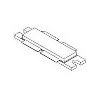
... N 1.218 1.242 30.94 31. 0.120 0.130 3.05 3.30 R 0.355 0.365 9.01 9.27 S 0.365 0.375 9.27 9.53 aaa 0.013 REF 0.33 REF bbb 0.010 REF 0.25 REF ccc 0.020 REF 0.51 REF STYLE 1: PIN 1. DRAIN M 2. DRAIN 3. GATE 4. GATE 5. SOURCE MRF9180R6 9 ...
Page 10
... The following table summarizes revisions to this document. Revision Date • Data sheet archived. Part no longer manufactured. 10 Dec. 2009 MRF9180R6 10 REVISION HISTORY Description RF Device Data Freescale Semiconductor ...
Page 11
... Denver, Colorado 80217 1-800-441-2447 or +1-303-675-2140 Fax: +1-303-675-2150 LDCForFreescaleSemiconductor@hibbertgroup.com RF Device Data Document Number: MRF9180 Rev. 10, 5/2006 Freescale Semiconductor Information in this document is provided solely to enable system and software implementers to use Freescale Semiconductor products. There are no express or implied copyright licenses granted hereunder to design or fabricate any integrated circuits or integrated circuits based on the information in this document ...