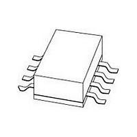
BLF202 NXP Semiconductors, BLF202 Datasheet - Page 6

BLF202
Manufacturer Part Number
BLF202
Description
Manufacturer
NXP Semiconductors
Datasheet
1.BLF202.pdf
(14 pages)
Specifications of BLF202
Application
HF/VHF
Channel Type
N
Channel Mode
Enhancement
Continuous Drain Current
1A
Drain Source Voltage (max)
40V
Output Power (max)
2W
Power Gain (typ)@vds
13@12.5VdB
Frequency (max)
175MHz
Package Type
CDIP SMD
Pin Count
8
Forward Transconductance (typ)
0.135S
Drain Source Resistance (max)
4000@15Vmohm
Input Capacitance (typ)@vds
5.3@12.5VpF
Output Capacitance (typ)@vds
7.8@12.5VpF
Reverse Capacitance (typ)
1.8@12.5VpF
Operating Temp Range
-65C to 200C
Drain Efficiency (typ)
55%
Mounting
Surface Mount
Mode Of Operation
CW Class-B
Number Of Elements
1
Power Dissipation (max)
5700mW
Vswr (max)
50
Screening Level
Military
Lead Free Status / Rohs Status
Compliant
Available stocks
Company
Part Number
Manufacturer
Quantity
Price
Part Number:
BLF202
Manufacturer:
NXP/恩智浦
Quantity:
20 000
Company:
Part Number:
BLF202,115
Manufacturer:
Wantcom
Quantity:
1 400
Philips Semiconductors
APPLICATION INFORMATION FOR CLASS-B OPERATION
T
RF performance in CW operation in a common source class-B test circuit.
Ruggedness in class-B operation
The BLF202 is capable of withstanding a load mismatch corresponding to VSWR = 50:1 through all phases under the
following conditions: V
2003 Sep 19
handbook, halfpage
CW, class-B
MODE OF OPERATION
mb
HF/VHF power MOS transistor
V
Fig.7
= 25 C; R
GS
(pF)
C rs
= 0; f = 1 MHz.
5
4
3
2
1
0
0
Feedback capacitance as a function of
drain-source voltage; typical values.
GS
= 237 ; unless otherwise specified.
4
DS
= 15.5 V; f = 175 MHz at rated load power.
8
(MHz)
175
f
12
V DS (V)
MGP115
12.5
V
16
(V)
DS
6
(mA)
I
20
DQ
(W)
P
2
L
typ. 13
(dB)
G
10
p
Product specification
BLF202
typ. 55
(%)
50
D


