HV5222PJ Supertex, HV5222PJ Datasheet
HV5222PJ
Specifications of HV5222PJ
Available stocks


Related parts for HV5222PJ


HV5222PJ Summary of contents
Page 1
Serial to Parallel Converter Features ► Processed with HVCMOS technology ® ► Output voltages to 225V using a ramped supply voltage ► SINK current minimum 100mA ► Shift register speed 8.0MHz ► Strobe and enable inputs ► CMOS compatible ...
Page 2
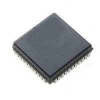
... Quad Plastic Gullwing (PG 44-Lead Quad Plastic Chip Carrier (PJ) Top Marking YY = Year Sealed YYWW WW = Week Sealed HV5222PJ L = Lot Number LLLLLLLLLL C = Country of Origin* Bottom Marking A = Assembler ID* = “Green” Packaging CCCCCCCCCCC AAA *May be part of top marking 44-Lead Quad Plastic Chip Carrier (PJ) ...
Page 3
Recommended Operating Conditions Sym Parameter V Logic voltage supply DD HV High voltage output OUT V High-level input voltage IH V Low-level input voltage IL f Clock frequency CLK T Operating free-air temperature A Power-Up Sequence Power-up sequence should be ...
Page 4
Input and Output Equivalent Circuits VDD Input GND Logic Inputs Switching Waveforms Data In Clock 50% Data Out Data Out Strobe HV OUT Function Table Function Data All on X All off X Load S Output Enable ...
Page 5
PQFP Pin Assignment (PG) HV5222PG Pin Function Description OUT OUT OUT OUT OUT OUT OUT ...
Page 6
... Pin Function Description 34 N/C No connect OUT OUT OUT OUT OUT High voltage outputs OUT OUT OUT OUT OUT 44-Lead PLCC Pin Assignment (DJ/PJ) HV5222PJ Pin Function Description OUT OUT OUT OUT OUT OUT OUT OUT High voltage outputs. OUT OUT OUT ...
Page 7
... PLCC Pin Assignment (PJ) HV5222PJ Pin Function Description 19 20 N/C No connect Output enable input When OE is LOW, all HV outputs are forced into a LOW state, regardless of data in each channel. When OE is HIGH, all HV outputs reflect data latched. Data shift register clock. 24 CLK Input are shifted into the shift register on the positive edge of the clock ...
Page 8
... A Pin 1 identifier must be located in the index area indicated. The Pin 1 identifier can be: a molded mark/identifier; an embedded metal marker printed indicator. Symbol A MIN .155 Dimension NOM .172 (inches) MAX .190 JEDEC Registration MO-087, Variation AB, Issue B, August, 1991. Drawings not to scale. Supertex Doc. #: DSPD-44CERPACDJ, Version D090808 Note 1 (Index Area) E1 Top View View B Seating Plane A1 ...
Page 9
... Dimension NOM - - (mm) MAX 2.35 0.25 JEDEC Registration MO-112, Variation AA-2, Issue B, Sep.1995. * This dimension is not specified in the original JEDEC drawing. The value listed is for reference only. Drawings not to scale. Supertex Doc. #: DSPD-44PQFPPG, Version A090808 View B Seating Plane 1.95 ...
Page 10
... Supertex Doc. #: DSPD-44PLCCPJ, Version D092408. Supertex inc. does not recommend the use of its products in life support applications, and will not knowingly sell them for use in such applications unless it receives an adequate “product liability indemnification insurance agreement.” Supertex inc. does not assume responsibility for use of devices described, and limits its liability to the replacement of the devices determined defective due to workmanship ...