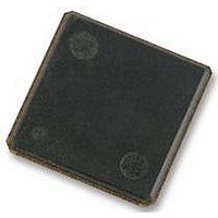
H5PS1G83EFR-S6C HYNIX SEMICONDUCTOR, H5PS1G83EFR-S6C Datasheet - Page 27

H5PS1G83EFR-S6C
Manufacturer Part Number
H5PS1G83EFR-S6C
Description
58T1895
Manufacturer
HYNIX SEMICONDUCTOR
Datasheet
1.H5PS1G83EFR-S6C.pdf
(44 pages)
Specifications of H5PS1G83EFR-S6C
Memory Type
SDRAM
Memory Configuration
128M X 8
Access Time
15ns
Memory Case Style
FBGA
No. Of Pins
60
Operating Temperature Range
0°C To +85°C
Memory Size
1 Gbit
Rohs Compliant
Yes
Available stocks
Company
Part Number
Manufacturer
Quantity
Price
Company:
Part Number:
H5PS1G83EFR-S6C
Manufacturer:
HYNIX
Quantity:
4 000
Part Number:
H5PS1G83EFR-S6C
Manufacturer:
HYNIX/海力士
Quantity:
20 000
Company:
Part Number:
H5PS1G83EFR-S6C-C
Manufacturer:
HYNIX
Quantity:
9 500
Company:
Part Number:
H5PS1G83EFR-S6C-C
Manufacturer:
HYNIX
Quantity:
135
Company:
Part Number:
H5PS1G83EFR-S6C-C-6Z
Manufacturer:
HYNIX
Quantity:
5 361
Rev. 0.4 / Nov 2008
4. Differential data strobe
DDR2 SDRAM pin timings are specified for either single ended mode or differential mode depending on the
setting of the EMR “Enable DQS” mode bit; timing advantages of differential mode are realized in system
design. The method by which the DDR2 SDRAM pin timings are measured is mode dependent. In single
ended mode, timing relationships are measured relative to the rising or falling edges of DQS crossing at VREF.
In differential mode, these timing relationships are measured relative to the crosspoint of DQS and its com-
plement, DQS. This distinction in timing methods is guaranteed by design and characterization. Note that
when differential data strobe mode is disabled via the EMR, the complementary pin, DQS, must be tied exter-
nally to VSS through a 20 Ω to 10 KΩ resistor to insure proper operation.
5. AC timings are for linear signal transitions. See System Derating for other signal transitions.
6. All voltages referenced to VSS.
7. These parameters guarantee device behavior, but they are not necessarily tested on each device. They
may be guaranteed by device design or tester correlation.
8. Tests for AC timing, IDD, and electrical (AC and DC) characteristics, may be conducted at nominal refer-
ence/supply voltage levels, but the related specifications and device operation are guaranteed for the full
voltage range specified.
CK/CK
DQS/DQS
DQ
DQS/
DQS
DQ
DM
CK
CK
DQS
DQS
t
CH
t
t
RPRE
DQS
DQS
WPRE
Figure -- Data output (read) timing
V
V
IL
IH
(ac)
(ac)
t
DMin
DS
t
t
CL
DQSQmax
D
Figure -- Data input (write) timing
t
DQSH
V
V
IH
IL
(ac)
(ac)
t
DMin
t
DS
QH
D
Q
t
DQSL
DMin
Q
D
t
DH
V
IH
V
(dc)
IL
(dc)
t
DQSQmax
DMin
Q
V
D
t
IL
DH
(dc)
V
IH
t
WPST
(dc)
t
t
RPST
QH
Q
H5PS1G43EFR
H5PS1G83EFR
H5PS1G63EFR
27


