DG411DJ+ Maxim Integrated Products, DG411DJ+ Datasheet - Page 4
DG411DJ+
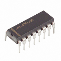
Manufacturer Part Number
DG411DJ+
Description
IC SWITCH QUAD SPST 16DIP
Manufacturer
Maxim Integrated Products
Type
Analog Switchr
Datasheet
1.DG412CUE.pdf
(12 pages)
Specifications of DG411DJ+
Function
Switch
Circuit
4 x SPST - NC
On-state Resistance
45 Ohm
Voltage Supply Source
Single, Dual Supply
Voltage - Supply, Single/dual (±)
5 V ~ 44 V, ±5 V ~ 20 V
Operating Temperature
0°C ~ 70°C
Mounting Type
Through Hole
Package / Case
16-DIP (0.300", 7.62mm)
Package
16PDIP N
Maximum On Resistance
80@10.8V Ohm
Maximum High Level Output Current
30 mA
Maximum Turn-off Time
145@±15V ns
Maximum Turn-on Time
250@12V ns
Switch Architecture
SPST
Power Supply Type
Single|Dual
Lead Free Status / RoHS Status
Lead free / RoHS Compliant


Improved, Quad,
SPST Analog Switches
ELECTRICAL CHARACTERISTICS—Single Supply
(V+ = 12V, V- = 0V, V
Note 2: The algebraic convention, where the most negative value is a minimum and the most positive value a maximum, is used in
Note 3: Guaranteed by design.
Note 4: ΔR
Note 5: Off-Isolation = 20log(V
Note 6: Between any two switches. See Figure 6.
Note 7: Leakage parameters I
4
SWITCH
SUPPLY
DYNAMIC
Analog Signal Range
Drain-Source On-Resistance
Positive Supply Current
Negative Supply Current
Logic Supply Current
Ground Current
Turn-On Time
Turn-Off Time
Break-Before-Make Time Delay
Charge Injection
(Note 3)
_______________________________________________________________________________________
PARAMETER
this data sheet.
bipolar-supply operation. Flatness is defined as the difference between the maximum and minimum value of on-resistance
as measured at the extremes of the specified analog signal range.
by correlation at +25°C.
ON
= ΔR
L
ON
= 5V, V
max - ΔR
GND
S(OFF)
D/
ON
V
= 0V, V
SYMBOL
V
S )
R
ANALOG
min. On-resistance match between channels and flatness are guaranteed only with
DS(ON)
I
, V
t
, I
GND
t
OFF
ON
I+
t
I
Q
I-
D
L
D(OFF)
D
= output, V
INH
, and I
= 2.4V, V
(Note 3)
V+ = 10.8V,
V
I
All channels on or off,
V+ = 13.2V,
V
All channels on or off,
V+ = 13.2V,
V
All channels on or off,
V
V
All channels on or off,
V
V
V
Figure 2
V
Figure 2
DG413 only,
R
Figure 3
C
V
R
Figure 4
S
D
IN
IN
L
IN
L
IN
S
S
L
GEN
L
GEN
= -10mA
= 300Ω, C
= 5.25V,
= 5.25V,
= 8V,
= 8V,
= 1.0nF,
= 3.8V,
= 0V or 5V
= 0V or 5V
= 0V or 5V
= 0V or 5V
D(ON)
= 0V,
S
= 0V,
= input to off switch. See Figure 5.
INL
are 100% tested at the maximum-rated hot temperature and guaranteed
= 0.8V, T
L
= 35pF,
CONDITIONS
A
= T
T
T
T
T
T
T
T
T
T
T
T
T
T
T
T
T
A
A
A
A
A
A
A
A
A
A
A
A
A
A
A
A
MIN
= +25°C
= T
= +25°C
= T
= +25°C
= T
= +25°C
= T
= +25°C
= T
= +25°C
= T
= +25°C
= T
= +25°C
= +25°C
to T
MIN
MAX
MAX
MAX
MAX
MIN
MIN
MAX
to T
to T
to T
, unless otherwise noted.)
MAX
MAX
MAX
MIN
-1
-5
-1
-5
-1
-5
-1
-5
0
(Note 2)
-0.0001
0.0001
0.0001
0.0001
TYP
175
40
95
25
5
MAX
100
250
315
125
140
12
80
10
5
1
1
1
5
1
5
5
UNITS
µA
µA
µA
µA
pC
ns
ns
ns
Ω
V
Related parts for DG411DJ+
Image
Part Number
Description
Manufacturer
Datasheet
Request
R

Part Number:
Description:
MAX7528KCWPMaxim Integrated Products [CMOS Dual 8-Bit Buffered Multiplying DACs]
Manufacturer:
Maxim Integrated Products
Datasheet:
Part Number:
Description:
Single +5V, fully integrated, 1.25Gbps laser diode driver.
Manufacturer:
Maxim Integrated Products
Datasheet:
Part Number:
Description:
Single +5V, fully integrated, 155Mbps laser diode driver.
Manufacturer:
Maxim Integrated Products
Datasheet:
Part Number:
Description:
VRD11/VRD10, K8 Rev F 2/3/4-Phase PWM Controllers with Integrated Dual MOSFET Drivers
Manufacturer:
Maxim Integrated Products
Datasheet:
Part Number:
Description:
Highly Integrated Level 2 SMBus Battery Chargers
Manufacturer:
Maxim Integrated Products
Datasheet:
Part Number:
Description:
Current Monitor and Accumulator with Integrated Sense Resistor; ; Temperature Range: -40°C to +85°C
Manufacturer:
Maxim Integrated Products
Part Number:
Description:
TSSOP 14/A�/RS-485 Transceivers with Integrated 100O/120O Termination Resis
Manufacturer:
Maxim Integrated Products
Part Number:
Description:
TSSOP 14/A�/RS-485 Transceivers with Integrated 100O/120O Termination Resis
Manufacturer:
Maxim Integrated Products
Part Number:
Description:
QFN 16/A�/AC-DC and DC-DC Peak-Current-Mode Converters with Integrated Step
Manufacturer:
Maxim Integrated Products
Part Number:
Description:
TDFN/A/65V, 1A, 600KHZ, SYNCHRONOUS STEP-DOWN REGULATOR WITH INTEGRATED SWI
Manufacturer:
Maxim Integrated Products
Part Number:
Description:
Integrated Temperature Controller f
Manufacturer:
Maxim Integrated Products
Part Number:
Description:
SOT23-6/I�/45MHz to 650MHz, Integrated IF VCOs with Differential Output
Manufacturer:
Maxim Integrated Products
Part Number:
Description:
SOT23-6/I�/45MHz to 650MHz, Integrated IF VCOs with Differential Output
Manufacturer:
Maxim Integrated Products
Part Number:
Description:
EVALUATION KIT/2.4GHZ TO 2.5GHZ 802.11G/B RF TRANSCEIVER WITH INTEGRATED PA
Manufacturer:
Maxim Integrated Products
Part Number:
Description:
QFN/E/DUAL PCIE/SATA HIGH SPEED SWITCH WITH INTEGRATED BIAS RESISTOR
Manufacturer:
Maxim Integrated Products
Datasheet: