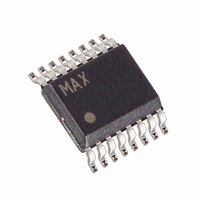
MAX3100CEE Maxim Integrated Products, MAX3100CEE Datasheet - Page 7

MAX3100CEE
Manufacturer Part Number
MAX3100CEE
Description
IC UART SPI/MICRWIRE COMP 16QSOP
Manufacturer
Maxim Integrated Products
Datasheet
1.MAX3100CEE.pdf
(24 pages)
Specifications of MAX3100CEE
Features
Low Power
Number Of Channels
1, UART
Fifo's
8 Byte
Protocol
RS232, RS485
Voltage - Supply
2.7 V ~ 5.5 V
With Irda Encoder/decoder
Yes
With False Start Bit Detection
Yes
With Cmos
Yes
Mounting Type
Surface Mount
Package / Case
16-SSOP (0.150", 3.90mm Width)
Lead Free Status / RoHS Status
Contains lead / RoHS non-compliant
Available stocks
Company
Part Number
Manufacturer
Quantity
Price
Company:
Part Number:
MAX3100CEE
Manufacturer:
MAXIM
Quantity:
44
Company:
Part Number:
MAX3100CEE
Manufacturer:
MAXIM
Quantity:
5 510
Part Number:
MAX3100CEE
Manufacturer:
MAXIM/美信
Quantity:
20 000
Company:
Part Number:
MAX3100CEE+
Manufacturer:
Maxim
Quantity:
15 139
Company:
Part Number:
MAX3100CEE+
Manufacturer:
Maxim
Quantity:
27
Company:
Part Number:
MAX3100CEE+T
Manufacturer:
Maxim
Quantity:
10 000
Part Number:
MAX3100CEE+T
Manufacturer:
MAXIM/美信
Quantity:
20 000
The receiver section receives data in serial form. The
MAX3100 detects a start bit on a high-to-low RX transi-
tion (Figure 3). An internal clock samples data at 16
times the data rate. The start bit can occur as much as
one clock cycle before it is detected, as indicated by
the shaded portion. The state of the start bit is defined
as the majority of the 7th, 8th, and 9th sample of the
internal 16x baud clock. Subsequent bits are also
majority sampled. Receive data is stored in an 8-word
FIFO. The FIFO is cleared if it overflows.
The on-board oscillator can use a 1.8432MHz or
3.6864MHz crystal, or it can be driven at X1 with a 45%
to 55% duty-cycle square wave.
Figure 3. Start-Bit Timing
Figure 4. SPI Interface (Write Configuration)
DOUT
SCLK
BLOCK
BAUD
DIN
CS
RX
1
R
A
1
1
_______________________________________________________________________________________
T
1
2
2
FEN
0
3
3
SHDN
0
4
4
TM
0
5
5
RM
0
6
6
PM
0
7
SPI/MICROWIRE-Compatible
7
RAM
0
8
ONE BAUD PERIOD
8
IR
0
9
9
The bit streams for DIN and DOUT consist of 16 bits,
with bits assigned as shown in the MAX3100
Operations section. DOUT transitions on SCLK’s falling
edge, and DIN is latched on SCLK’s rising edge (Figure
4). Most operations, such as the clearing of internal
registers, are executed only on CS’s rising edge. The
DIN stream is monitored for its first two bits to tell the
UART the type of data transfer being executed (Write
Config, Read Config, Write Data, Read Data).
Only 16-bit words are expected. If CS goes high in the
middle of a transmission (any time before the 16th bit),
the sequence is aborted (i.e., data does not get written
to individual registers). Every time CS goes low, a new
16-bit stream is expected. An example of a write con-
figuration is shown in Figure 4.
ST
0
10
10
MAJORITY
SAMPLER
CENTER
PE
0
11
11
0
L
UART in QSOP-16
12
12
B3
0
13
13
B2
0
14
14
B1
0
15
15
B0
0
16
16
UPDATED
SPI Interface
DATA
7


