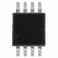
TS4994IST STMicroelectronics, TS4994IST Datasheet - Page 29

TS4994IST
Manufacturer Part Number
TS4994IST
Description
IC AMP AUDIO PWR 1W MONO 8MSOP
Manufacturer
STMicroelectronics
Type
Class ABr
Datasheet
1.TS4994IST.pdf
(35 pages)
Specifications of TS4994IST
Output Type
1-Channel (Mono)
Max Output Power X Channels @ Load
1W x 1 @ 8 Ohm
Voltage - Supply
2.5 V ~ 5.5 V
Features
Depop, Differential Inputs, Short-Circuit and Thermal Protection, Standby
Mounting Type
Surface Mount
Package / Case
8-MSOP, Micro8™, 8-uMAX, 8-uSOP,
For Use With
497-6396 - BOARD EVAL FOR LV TS4984IQT497-6395 - BOARD EVAL FOR LP DIFF TS4994IQT
Lead Free Status / RoHS Status
Lead free / RoHS Compliant
Other names
497-4452-2
Available stocks
Company
Part Number
Manufacturer
Quantity
Price
Part Number:
TS4994IST
Manufacturer:
ST
Quantity:
20 000
TS4994
4.10
Note:
4.11
4.12
Shutdown time
When the standby command is set, the time required to put the two output stages in high
impedance and the internal circuitry in shutdown mode is a few microseconds.
In shutdown mode, the Bypass pin and Vin+, Vin- pins are short-circuited to ground by
internal switches. This allows a quick discharge of the C
Pop performance
Due to its fully differential structure, the pop performance of the TS4994 is close to perfect.
However, due to mismatching between internal resistors R
capacitors C
components, the TS4994 includes pop reduction circuitry. With this circuitry, the TS4994 is
close to zero pop for all possible common applications.
In addition, when the TS4994 is in standby mode, due to the high impedance output stage in
this configuration, no pop is heard.
Single-ended input configuration
It is possible to use the TS4994 in a single-ended input configuration. However, input
coupling capacitors are needed in this configuration. The schematic in
configuration using the MiniSO-8 version of the TS4994 as an example.
Figure 79. Single-ended input typical application
GND
Ve
in
Optional
220nF
220nF
, some noise might remain at startup. To eliminate the effect of mismatched
Cin1
Cin2
Rin1
20k
Rin2
20k
+
GND
Cb
1u
2
3
4
Rfeed1
20k
Vin-
Vin+
Bypass
GND VCC
Stdby
1
7
VCC
GND
6
GND
VCC
Standby
-
+
Bias
b
and C
in
Rfeed2
20k
+
, R
GND
feed
Cs
1u
in
capacitors.
, and external input
Application information
TS4994IS
Figure 79
Vo+
Vo-
8
5
shows this
8 Ohms
29/35


