STA50813TR STMicroelectronics, STA50813TR Datasheet
STA50813TR
Specifications of STA50813TR
STA50813TR
Available stocks


Related parts for STA50813TR


STA50813TR Summary of contents
Page 1
FEATURES MULTIPOWER BCD TECHNOLOGY ■ MINIMUM INPUT OUTPUT PULSE WIDTH ■ DISTORTION 200mΩ R COMPLEMENTARY DMOS ■ dsON OUTPUT STAGE CMOS COMPATIBLE LOGIC INPUTS ■ THERMAL PROTECTION ■ THERMAL WARNING OUTPUT ■ UNDER VOLTAGE PROTECTION ■ 2 DESCRIPTION STA508 ...
Page 2
STA508 Table 2. Pin Description N° Pin 1 GND-SUB Substrate Ground OUT2B Output Half Bridge Positive Supply CC 5 GND2B Negative Supply 6 GND2A Negative Supply Positive Supply CC 8 ...
Page 3
Table 3. FUNCTIONAL PIN STATUS PIN NAME FAULT (*) FAULT TRI-STATE TRI-STATE PWRDN PWRDN THWAR (*) THWAR CONFIG (**) CONFIG (*) : The pin is open collector. To have the high logic value, it needs to be pulled up by ...
Page 4
STA508 Table 5. ABSOLUTE MAXIMUM RATINGS Symbol V DC Supply Voltage (Pin 4,7,12,15 Maximum Voltage on pins max P Power Dissipation (T tot T Operating Temperature Range Storage and Junction Temperature ...
Page 5
Table 6. ELECTRICAL CHARACTERISTCS (continued) Symbol Parameter V High logical state voltage VH (pin H PWRDN, TRISTATE) (note 1) I Supply CURRENT from Vcc in VCC- Power Down PWRDN I Output Current pins FAULT FAULT -TH-WARN when FAULT CONDITIONS I ...
Page 6
STA508 Figure 4. Test Circuit. Low current dead time = MAX(DTr,DTf) Duty cycle = 50% INxY Figure 5. INxA Figure 6. High Current Dead time for Bridge application = ABS(DTout(A)-DTin(A))+ABS(DTOUT(B)-DTin(B)) Duty cycle=A M58 DTin(A) INA M57 Duty cycle A and ...
Page 7
Figure 7. Typical Single BTL Configuration V L +3.3V 100nF GND-Clean GND-Reg 100nF 10K X7R CONFIG TH_WAR TH_WAR PWRDN nPWRDN FAULT 10K TRI-STATE 100nF IN1A IN1B IN1A IN2A IN2B IN1B 100nF V ...
Page 8
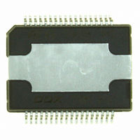
STA508 Figure 9. Power SO36 (SLUG UP) Mechanical Data & Package Dimensions MIN. TYP. MAX. A 3.25 3.43 A2 3.1 3 0.2 a1 0.030 -0.040 0.0011 b 0.22 0.38 c 0.23 0.32 D ...
Page 9
Table 9. Revision History Date Revision September 1994 June 2004 November 2004 February 2006 1 First Issue 2 Note 2: See relevant Application Note AN1994 3 Changed Vcc from 9 min to 10 min 4 Changed T value on Table ...
Page 10
... STA508 Information in this document is provided solely in connection with ST products. STMicroelectronics NV and its subsidiaries (“ST”) reserve the right to make changes, corrections, modifications or improvements, to this document, and the products and services described herein at any time, without notice. All ST products are sold pursuant to ST’s terms and conditions of sale. ...