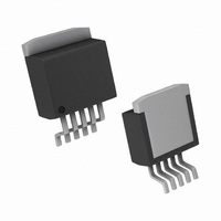
LME49600TS/NOPB National Semiconductor, LME49600TS/NOPB Datasheet - Page 10

LME49600TS/NOPB
Manufacturer Part Number
LME49600TS/NOPB
Description
IC AMP BUFFER AUD HI FI TO-263-5
Manufacturer
National Semiconductor
Type
Class ABr
Datasheet
1.LME49600TSNOPB.pdf
(20 pages)
Specifications of LME49600TS/NOPB
Output Type
1-Channel (Mono)
Max Output Power X Channels @ Load
500mW x 1 @ 32 Ohm
Voltage - Supply
±2.25 V ~ 18 V
Features
Short-Circuit and Thermal Protection
Mounting Type
Surface Mount
Package / Case
D²Pak, TO-263 (5 leads + tab)
Amplifier Class
AB
No. Of Channels
1
Supply Voltage Range
± 2.25V To ± 18V
Load Impedance
32ohm
Operating Temperature Range
-40°C To +85°C
Amplifier Case Style
TO-263
No. Of Pins
5
Rohs Compliant
Yes
Number Of Channels
1
Voltage Gain Db
0.09 dB
Input Voltage Range (max)
36 V
Input Voltage Range (min)
4.5 V
Input Offset Voltage
60 mV at +/- 15 V
Supply Current
14.5 mA
Maximum Operating Temperature
+ 85 C
Mounting Style
SMD/SMT
Maximum Dual Supply Voltage
+/- 18 V
Minimum Operating Temperature
- 40 C
Lead Free Status / RoHS Status
Lead free / RoHS Compliant
Other names
*LME49600TS/NOPB
LME49600TS
LME49600TS
www.national.com
Application Information
HIGH PERFORMANCE, HIGH FIDELITY HEADPHONE
AMPLIFIER
The LME49600 is the ideal solution for high output, high per-
formance high fidelity head phone amplifiers. When placed in
the feedback loop of the LME49710, LME49720 or
LME49740 High Performance, High Fidelity audio operational
amplifier, the LME49600 is able to drive 32Ω headphones to
a dissipation of greater than 500mW at 0.00003% THD+N
while operating on ±15V power supply voltages. The circuit
schematic for a typical headphone amplifier is shown in Fig-
ure 4.
Operation
The following describes the circuit operation for the head-
phone amplifier’s Left Channel. The Right Channel operates
identically.
FIGURE 3. THD+N Distortion Test Circuit
10
The audio input signal is applied to the input jack (HP31 or
J1/J2) and dc-coupled to the volume control, VR1. The output
signal from VR1’s wiper is applied to the non-inverting input
of U2-A, an LME49720 High Performance, High Fidelity audio
operational amplifier. U2-A’s AC signal gain is set by resistors
R2, R4, and R6. To allow for a DC-coupled signal path and to
ensure minimal output DC voltage regardless of the closed-
loop gain, the other half of the U2 is configured as a DC servo.
By constantly monitoring U2-A’s output, the servo creates a
voltage that compensates for any DC voltage that may be
present at the output. A correction voltage is generated and
applied to the feedback node at U2-A, pin 2. The servo en-
sures that the gain at DC is unity. Based on the values shown
in Figure 4, the RC combination formed by R11 and C7 sets
the servo’s high-pass cutoff at 0.16Hz. This is over two
decades below 20Hz, minimizing both amplitude and phase
perturbations in the audio frequency band’s lowest frequen-
cies.
30029843


