LM49350RL/NOPB National Semiconductor, LM49350RL/NOPB Datasheet
LM49350RL/NOPB
Specifications of LM49350RL/NOPB


Related parts for LM49350RL/NOPB


LM49350RL/NOPB Summary of contents
Page 1
... LS_V and A_V = 2. I/O_V = 1.6V to 4.5V DD Boomer® registered trademark of National Semiconductor Corporation. © 2009 National Semiconductor Corporation LM49350 ■ SNR (Stereo DAC at 48kHz) ■ SNR (Stereo ADC at 48kHz) ■ Shutdown Current ■ PSRR at 217 Hz, A_V AUX) 4 ...
Page 2
LM49350 Overview www.national.com FIGURE 1. LM49350 Block Diagram 2 20194111 ...
Page 3
Typical Application FIGURE 2. Example Application in Multimedia Phone with a Dedicated Earpiece and Mono Loudspeaker 3 20194102 www.national.com ...
Page 4
FIGURE 3. Example Application in Multimedia Phone Using Stereo Loudspeaker www.national.com 4 20194103 ...
Page 5
FIGURE 4. Example Application in a Multimedia Phone Using a Dedicated RF Module for Voice Modern Functions 5 20194104 www.national.com ...
Page 6
FIGURE 5. Example Application in a Portable Media Player with a Differential Stereo Line Input www.national.com 6 20194105 ...
Page 7
General Description ......................................................................................................................... 1 2.0 Applications .................................................................................................................................... 1 3.0 Key Specifications ........................................................................................................................... 1 4.0 Features ........................................................................................................................................ 1 5.0 LM49350 Overview .......................................................................................................................... 2 6.0 Typical Application ........................................................................................................................... 3 7.0 Connection Diagrams ..................................................................................................................... 10 7.1 PIN TYPE DEFINITIONS ........................................................................................................ 11 8.0 ...
Page 8
FIGURE 15. EMI/RFI Filter for the Class D Amplifier ......................................................................................... 43 FIGURE 16. Digital Mixer .......................................................................................................................... 51 FIGURE 17 Serial Data Format (24 bit example) ........................................................................................ 55 2 FIGURE 18. Left Justified Data Format (24 bit example) .................................................................................... ...
Page 9
TABLE 51. ADC_ALC_4 (0x84h) ................................................................................................................. 65 TABLE 52. ADC_ALC_5 (0x85h) ................................................................................................................. 66 TABLE 53. ADC_ALC_6 (0x86h) ................................................................................................................. 67 TABLE 54. ADC_ALC_7 (0x87h) ................................................................................................................. 67 TABLE 55. ADC_ALC_8 (0x88h) ................................................................................................................. 67 TABLE 56. ADC_L_LEVEL (0x89h) (Default data value is 0x33h) ......................................................................... ...
Page 10
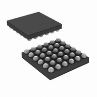
Connection Diagrams 36 Bump micro SMD Top View (Bump Side Down) Order Number LM49350RL See NS Package Number RLA36TTA Ordering Information Order Number Package 36 Bump micro LM49350RL SMDxt 36 Bump micro LM49350RLX SMDxt www.national.com 20194101 Package DWG # ...
Page 11
Pin Descriptions Pin Pin Name Type Direction A1 HPR Analog A2 A_V Supply DD A3 AGND Supply A4 VREF_FLT Analog Input/Output A5 GPIO Digital Input/Output A6 SDA Digital Input/Output B1 HPL Analog B2 AUX_R Analog B3 AUX_L Analog B4 PORT2_SYNC ...
Page 12
... Absolute Maximum Ratings Military/Aerospace specified devices are required, please contact the National Semiconductor Sales Office/ Distributors for availability and specifications. Analog Supply Voltage (A_V and LS_V ) DD DD Digital Supply Voltage D_V DD I/O Supply Voltage I/O_V DD Storage Temperature Power Dissipation (Note ) ...
Page 13
Symbol Parameter MICI Microphone Quiescent Current DD ADCI ADC Total Active Current DD DACI DAC Total Active Current DD Auxiliary Input Amplifier Quiescent AUXINI DD Current Auxiliary Output Amplifier Quiescent AUXOUTI DD Current LOUDSPEAKER AMPLIFIER LS Loudspeaker Efficiency EFF THD+N ...
Page 14
Symbol Parameter e Output Noise OS X Crosstalk TALK ΔA Channel-to-Channel Gain Matching CH-CH V Output Offset Voltage OS T Turn-On Time WU AUXILIARY OUTPUTS THD+N Total Harmonic Distortion + Noise P Output Power OUT PSRR Power Supply Rejection Ratio ...
Page 15
Symbol Parameter ADC ADC Full Scale Input Level LEVEL STEREO DAC DAC Total Harmonic Distortion + THD+N DAC Noise DAC DAC Full Scale Output Level LEVEL R DAC Ripple DAC PB DAC Passband DAC SNR DAC Signal-to-Noise Ratio DAC MIC ...
Page 16
Timing Characteristics 8Ω 32Ω 1kHz, unless otherwise specified. Limits apply for T apply for R L(SP) L(HP) Symbol Parameter PLL f PLL Input Frequency Range IN DIGITAL AUDIO INTERFACE TIMING t BCK rise ...
Page 17
Typical Performance Characteristics DAC Frequency Response f = 48kHz, OSR = 128 S Stereo Audio ADC Frequency Response = 1μF, MIC gain = 6dB f = 48kHz, OSR = 128 Stereo Audio ADC HPF Frequency Response ...
Page 18
Mono Voice ADC Frequency Response = 1μF, MIC gain = 6dB f = 8kHz, OSR = 128 Mono Voice ADC HPF Frequency Response = 1μF, MIC gain = 6dB f = 8kHz, OSR = 128 ...
Page 19
ADC Output THD Differential MIC Input, MIC Gain = 6dB V = 1kHz 48kHz IN S 20194149 Loudspeaker THD+N vs Frequency Differential Aux Input, Aux Gain = 0dB = 8Ω 5V ...
Page 20
Loudspeaker THD+N vs Output Power Differential Aux Input, Aux Gain = 0dB 1kHz Loudspeaker THD+N vs Output Power Differential Aux Input, Aux Gain = 0dB = 4Ω 1kHz LS_V = ...
Page 21
Loudspeaker PSRR vs Frequency LS_V = 5V, Aux Gain = 0dB DD Differential Aux Input to Ground V = 200mV RIPPLE PP 20194153 Headphone THD+N vs Frequency Stereo Aux Input, Aux Gain = 0dB = 32Ω 5V, P ...
Page 22
Headphone THD+N vs Output Power A_V = 3.3V, Stereo Aux Input, Aux Gain = 0dB DD = 16Ω 1kHz R L Headphone Crosstalk vs Frequency Stereo Aux Inputs, Aux Gain = 0dB, R Earpiece THD+N vs Output Power ...
Page 23
AUXOUT THD+N vs Frequency Differential Aux Input, Aux Gain = 0dB 5kΩ DD OUT RMS L AUXOUT PSRR vs Frequency Differential Aux Input to Ground, Aux Gain = 0dB V = ...
Page 24
System Control Method Compatible Interface 13 SIGNALS mode the LM49350 pin SCL is used for the I SCL and the pin SDA is used for the I 13.3 ...
Page 25
FIGURE 9. Example Write Cycle 25 20194126 www.national.com ...
Page 26
When a READ function accomplished, a WRITE function must precede the READ function, as shown in the Read Cycle waveform. 13 TIMING PARAMETERS Symbol 1 Hold Time (repeated) START Condition 2 Clock Low Time ...
Page 27
Device Register Map Address Register 7 0x00h PMC CHIP SETUP ACTIVE 0x01h PMC CLOCKS 0x02h PMC CLK_DIV 0x03h 0x04h PLL1 M 0x05h PLL1 N 0x06h PLL1 N_MOD 0x07h PLL1 P1 0x08h PLL1 P2 0x09h PLL2 M 0x0Ah PLL2 N ...
Page 28
Address Register 7 0x31h DAC_CLO CK 0x32h DAC_DSP 0x40h IPLVL1 PORT2_RX_R_LVL 0x41h IPLVL2 INTERP_L_LVL 0x42h OPPORT1 0x43h OPPORT2 0x44h OPDAC 0x45h OPDECI 0x50h BASIC STEREO_ SYNC_MO DE 0x51h CLK_GEN 1 0x52h CLK_GEN 2 0x53h SYNC_GE N 0x54h DATA_WI TX_EXTRA_BITS DTH ...
Page 29
Address Register 7 0x82h ADC ALC 2 0x83h ADC ALC 3 0x84h ADC ALC 4 0x85h ADC PK_DECAY_RATE ALC 5 0x86h ADC ALC 6 0x87h ADC ALC 7 0x88h ADC ALC 8 0x89h ADC L LEVEL 0x8Ah ADC R LEVEL ...
Page 30
Address Register 7 0xA4h DAC ALC 5 0xA5h DAC ALC 6 0xA6h DAC ALC 7 0xA7h DAC ALC 8 0xA8h DAC L LEVEL 0xA9h DAC R LEVEL 0xAAh DAC_3D ATTEN 0xABh EQ BAND 1 0xACh EQ BAND Q 2 0xADh ...
Page 31
Address Register 7 0xFBh ADC_C1_ MSB 0xFCh ADC_C2_L SB 0xFDh ADC_C2_ MSB 0xFEh AUX_LINE _OUT Unless otherwise specified, the default values of the I isters is 0x00h ADC_C1_MSB ADC_C2_LSB ADC_C2_MSB AUX_LINE _OUT 2 C reg- 31 ...
Page 32
Basic PMC Setup Register This register is used to control the LM49350's Basic Power Management Setup: Bits Field 0 CHIP_ENABLE 1 PLL1_ENB 2 PLL2_ENB 3 OSC_ENB 4 MCLK_OVR 5 PORT1_CLK_OVR 6 PORT2_CLK_OVR 7 CHIP_ACTIVE 1. If the PMC is ...
Page 33
PMC Clocks Register This register is used to control the LM49350's Basic Power Management Setup: Bits Field 1:0 PMC_CLK_SEL 17.0 PMC Clock Divide Register This register is used to control the LM49350's Power Management Circuits Clocks: TABLE 4. PMC_SETUP ...
Page 34
LM49350 Clock Network (Refer to Figure 12) The audio DAC and ADC operate at a clock frequency of 2*OSR*f where OSR is the oversampling ratio and f S sampling frequency of the DAC or ADC. The DAC can operate ...
Page 35
FIGURE 12. Internal Clock Network 35 20194129 www.national.com ...
Page 36
PLL Setup Registers The LM49350 contains two PLLs for flexible operation of its dual audio ports. PLL1 has a P1 and P2 output divider thereby allowing PLL1 to generate two distinct clock outputs. The equations for PLL1's generated output ...
Page 37
TABLE 7. PLL Settings for Common System Clock Frequencies f (MHz 2 15.5 175 14.4 12.5 128 16.2 13.5 128 16.8 3.5 32 19.2 12.5 96 19.68 20.5 160 19.8 16.5 128 27 22.5 ...
Page 38
Bits Field 1:0 PLL1_CLK_SEL Bits Field 6:0 PLL1_M Bits Field 7:0 PLL1_N www.national.com TABLE 8. PLL_CLOCK_SOURCE (0x03h) This selects the source of the input clock to PLL1 PLL1_CLK_SEL TABLE 9. PLL1_M (0x04h) This programs the PLL1 ...
Page 39
Bits Field 4:0 PLL1_N_MOD This programs the sigma-delta modulator in PLL1 5 PLL1_P1[8] This sets the MSB of the 1st P Divider on PLL1 which is part of a standard half-cycle divider control. 6 PLL1_P2[8] This sets the MSB of ...
Page 40
Bits Field 6:0 PLL2_M Bits Field 7:0 PLL2_N Bits Field 4:0 PLL2_N_MOD 5 PLL2_P[8] www.national.com TABLE 14. PLL2_M (0x09h) This programs the PLL2 M divider to divide from 1 to 64. PLL2_M 0000000 0000001 0000010 0000011 0000100 0000101 — 1111101 ...
Page 41
Bits Field 7:0 PLL2_P[7:0] This programs the 8 LSBs of PLL2's P Divider. These LSBs combine with PLL2_P[8] which allows the P divider to divide 256 TABLE 17. PLL2_P (0x0Ch) Description PLL2_P 000000000 000000001 000000010 000000011 000000100 ...
Page 42
Analog Mixer Control Registers This register is used to control the LM49350's Analog Mixer: Bits Field 0 DACR_LS 1 DACL_LS 2 MICR_LS 3 MICL_LS 4 AUXR_LS 5 AUXL_LS 20.1 CLASS D LOUDSPEAKER AMPLIFIER The LM49350 features a filterless modulation ...
Page 43
FIGURE 15. EMI/RFI Filter for the Class D Amplifier TABLE 19. LEFT HEADPHONE_OUTPUT (0x11h) Bits Field 0 DACR_HPL The right DAC output is added to the left headphone output. 1 DACL_HPL The left DAC output is added to the left ...
Page 44
Please refer to the demonstration board schematic shown in Figure 23. Bits Field 0 DACR_AUX 1 DACL_AUX 2 MICR_AUX 3 MICL_AUX 4 AUXR_AUX 5 AUXL_AUX 20.8 AUXILIARY OUTPUT AMPLIFIER The LM49350’s auxiliary output (AUXOUT) amplifier provides differential drive ...
Page 45
Bits Field 3:0 MIC_L_LEVEL This sets the gain of the left microphone preamp. 4 SE_DIFF If set, the MIC_L negative input is ignored. 5 MUTE If set, the left microphone preamp is muted. Bits Field 3:0 MIC_R_LEVEL This sets the ...
Page 46
Bits Field 5:0 AUX_L_LEVEL This programs the left AUX input level. All gain changes are performed at zero crossings. AUX_L_LEVEL 000000 000001 000010 000011 000100 000101 000110 000111 001000 001001 001010 001011 001100 001101 001110 001111 010000 010001 010010 010011 ...
Page 47
Bits Field 5:0 AUX_R_LEVEL This programs the right AUX input level. All gain changes are performed at zero crossings. AUX_R_LEVEL 000000 000001 000010 000011 000100 000101 000110 000111 001000 001001 001010 001011 001100 001101 001110 001111 010000 010001 010010 010011 ...
Page 48
ADC Control Registers This register is used to control the LM49350's ADC: Bits Field 0 MONO This sets mono or stereo operation of the ADC. 1 OSR This sets the oversampling ratio of the ADC. 2 MUTE_L If set, ...
Page 49
Bits Field 7:0 ADC_TRIM If set, the ADC is compensated with recommended compensation filter coefficients. The recommended ADC compensation filter coefficients are programmed as follows: TABLE 30. ADC TRIM (0x22h) Description Register 0xF8h set to 0x00h Register 0xF9h set to ...
Page 50
DAC Control Registers This register is used to control the LM49350's DAC: Bits Field 1:0 MODE This programs the over sampling ratio of the stereo DAC. 2 MUTE_L This digitally mutes the Left DAC output. 3 MUTE_R This digitally ...
Page 51
Digital Mixer Control Registers 23.1 DIGITAL MIXER The LM49350’s digital mixer allows for flexible routing of dig- ital audio signals between both audio ports, DAC, and ADC. This mixer handles which digital data path (Port1 RX data, Port2 RX ...
Page 52
This register is used to control the LM49350's digital mixer: Bits Field 1:0 PORT1_RX_L This programs the input level of the data arriving from the left receive channel of Audio Port 1. _LVL 3:2 PORT1_RX_R This programs the input level ...
Page 53
Bits Field 7:6 INTERP_R_LVL This programs the input level of the data arriving from the right DAC's interpolator output. Bits Field 1:0 L_SEL This selects which input is fed to the Left TX Channel of Audio Port 1. 3:2 R_SEL ...
Page 54
Bits Field 0 PORT1_L This adds Audio Port 1's left RX channel to the DAC's left input. 1 PORT2_L This adds Audio Port 2's left RX channel to the DAC's left input. 2 ADC_L This adds the ADC's left output ...
Page 55
Audio Port Control Registers FIGURE 17. I FIGURE 18. Left Justified Data Format (24 bit example) FIGURE 19. Right Justified Data Format (24 bit example) FIGURE 20. PCM Serial Data Format (16 bit example Serial Data Format ...
Page 56
The following registers are used to control the LM49350's audio ports. Audio Port 1 and Audio Port 2 are identical. Port 1 is programmed through the (0x5Xh) registers. Port 2 is programmed through the (0x6Xh) registers. Bits Field 0 STEREO ...
Page 57
Bits Field 2:0 SYNTH_NUM Along with SYNTH_DENOM, this sets the clock divider that generates the Port 1 or Port 2 clock in master mode. SYNTH_NUM 3 SYNTH_DENOM Along with SYNTH_NUM, this sets the clock divider that generates the Port 1 ...
Page 58
Bits Field 5:3 SYNC_WIDTH In MONO mode, this programs the width (in number of bits) of the SYNC signal. Bits Field 2:0 RX_WIDTH This programs the expected bits per word of the serial data input SDI. 5:3 TX_WIDTH This programs ...
Page 59
Bits Field 0 TX_MODE This sets the TX data input justification with respect to the SYNC signal. 5:1 MSB_POSITION This specifies the bit location of the MSB from the start of the frame (MSB Justified) or from the end of ...
Page 60
Digital Effects Engine 25.1 DIGITAL SIGNAL PROCESSOR (DSP) The LM49350 is designed to handle the entire audio signal conditioning and processing within the audio system, thereby freeing up the workload of any other applications processor contained within the system. ...
Page 61
Bits Field 2:0 HPF_MODE This configures the ADC's High Pass Filter. TABLE 47. HPF MODE (0x80h) Description HPF_MODE 000 001 010 011 100 101 110 111 61 FILTER CHARACTERISTICS 8kHz Voice 12kHz Voice 16kHz Voice 24kHz Voice 32kHz Voice 32kHz ...
Page 62
ALC OVERVIEW The Automatic Level Control (ALC) system can be used to regulate the audio output level to a user defined target level. The ALC feature is especially useful whenever the level of the audio input is unknown, unpredictable, ...
Page 63
Bits Field 3 LIMITER If set, the circuit will never apply gain to the signal, no matter how small, but it will attenuate the signal as soon as it reaches target and release it at the decay rate, once signal ...
Page 64
Bits Field 4:0 TARGET_LEVEL This sets the desired target output level. Signals lower than this will be amplified and signals larger than this will be attenuated. www.national.com TABLE 50. ADC_ALC_3 (0x83h) Description TARGET_LEVEL 00000 00001 00010 00011 00100 00101 00110 ...
Page 65
Bits Field 4:0 ATTACK_RATE This sets the rate at which the ALC will reduce gain if it detects the input signal is large. TABLE 51. ADC_ALC_4 (0x84h) Description ATTACK_RATE 00000 00001 00010 00011 00100 00101 00110 00111 01000 01001 01010 ...
Page 66
Bits Field 4:0 DECAY_RATE 7:5 PK_DECAY_RATE www.national.com TABLE 52. ADC_ALC_5 (0x85h) Description This sets the rate at which the ALC will increase gain if it detects the input signal is too small. DECAY_RATE 00000 00001 00010 00011 00100 00101 00110 ...
Page 67
TABLE 53. ADC_ALC_6 (0x86h) Bits Field 4:0 HOLD_TIME This sets how long the ALC circuit waits before increasing the gain. TABLE 54. ADC_ALC_7 (0x87h) Bits Field 5:0 MAX_LEVEL This sets the maximum allowed gain of the volume control to the ...
Page 68
TABLE 56. ADC_L_LEVEL (0x89h) (Default data value is 0x33h) Bits Field 5:0 ADC_L_LEVEL www.national.com Description This sets the post ADC digital gain of the left channel. ADC_L_LEVEL Level 000000 -76.5dB 000001 -75dB 000010 -73.5dB 000011 -72dB 000100 -70.5dB 000101 -69dB ...
Page 69
TABLE 57. ADC_R_LEVEL (0x8Ah) (Default data value is 0x33h) Bits Field 5:0 ADC_R_LEVEL This sets the post ADC digital gain of the right channel. ADC_R_LEVEL 000000 000001 000010 000011 000100 000101 000110 000111 001000 001001 001010 001011 001100 001101 001110 ...
Page 70
Bits Field 1:0 FREQ 6:2 LEVEL www.national.com TABLE 58. EQ_BAND_1 (0x8Bh) Description This sets the Sub-bass shelving filter's cut-off frequency. FREQ This sets the gain LEVEL 00000 00001 00010 00011 00100 00101 ...
Page 71
TABLE 59. EQ_BAND_2 (0x8Ch) Bits Field 1:0 FREQ This sets the Bass peak filter's center frequency. FREQ 6:2 LEVEL This sets the gain at fc. LEVEL 100000 100001 100010 100011 100100 100101 100110 100111 101000 101001 101010 101011 101100 101101 ...
Page 72
Bits Field 1:0 FREQ 6:2 LEVEL 7 Q www.national.com TABLE 60. EQ_BAND_3 (0x8Dh) Description This sets the Mid peak filter's center frequency. FREQ 100 101 110 111 This sets the gain at fc. LEVEL 00000 00001 00010 00011 00100 00101 ...
Page 73
TABLE 61. EQ_BAND_4 (0x8Eh) Bits Field 1:0 FREQ This sets the Treble peak filter's center frequency. FREQ 6:2 LEVEL This sets the gain at fc. LEVEL 00000 00001 00010 00011 00100 00101 00110 00111 01000 01001 01010 01011 01100 01101 ...
Page 74
Bits Field 1:0 FREQ 6:2 LEVEL www.national.com TABLE 62. EQ_BAND_5 (0x8Fh) Description This sets the presence shelving filter's cut-off frequency. FREQ This sets the gain at fc. LEVEL 00000 00001 00010 00011 00100 00101 00110 00111 ...
Page 75
TABLE 63. SOFTCLIP1 (0x90h) Bits Field 3:0 THRESHOLD This sets the threshold level of the audio compressor. Audio signals above the threshold will be compressed. THRESHOLD 4 SOFT_KNEE If set, the audio compressor will automatically apply higher compression ratios to ...
Page 76
Bits 4:0 www.national.com TABLE 64. SOFTCLIP2 (0x91h) Field Description RATIO This sets the ratio at which the audio is compressed to when it passes beyond the threshold. In SOFT_KNEE mode this is the final level of compression. RATIO 00000 00001 ...
Page 77
TABLE 65. SOFTCLIP3 (0x92h) Bits Field 4:0 LEVEL This sets the post compressor gain level. LEVEL 00000 00001 00010 00011 00100 00101 00110 00111 01000 01001 01010 01011 01100 01101 01110 01111 10000 10001 10010 10011 10100 10101 10110 10111 ...
Page 78
DAC Effects Registers Bits 2 www.national.com TABLE 66. DAC_ALC_1 (0xA0h) Field Description SAMPLE_ RATE This programs the timers on the ALC with the closest DAC sample rate. SAMPLE_ RATE 000 001 010 011 100 101 110 111 ...
Page 79
TABLE 67. DAC_ALC_2 (0xA1h) Bits Field 3:0 NOISE_FLOOR This sets the anticipated noise floor. Signals lower than the specified noise floor will be gated from the ALC to avoid noise pumping. NOISE_FLOOR 4 NG_ENB This enables the Noise Gate 79 ...
Page 80
Bits 4:0 www.national.com TABLE 68. DAC_ALC_3 (0xA2h) Field Description TARGET_LEVEL This sets the desired output level. Signals lower than this will be amplified and signals larger than this will be attenuated. TARGET_LEVEL Target Level (dB) 00000 00001 00010 00011 00100 ...
Page 81
TABLE 69. DAC_ALC_4 (0xA3h) Bits Field 4:0 ATTACK_RATE This sets the rate at which the ALC will reduce gain if it detects the input signal is too large. ATTACK_RATE 00000 00001 00010 00011 00100 00101 00110 00111 01000 01001 01010 ...
Page 82
Bits 4:0 7:5 www.national.com TABLE 70. DAC_ALC_5 (0xA4h) Field DECAY_RATE This sets the rate at which the ALC will increase gain if it detects the input signal is too small. DECAY_RATE 00000 00001 00010 00011 00100 00101 00110 00111 01000 ...
Page 83
TABLE 71. DAC_ALC_6 (0xA5h) Bits Field 4:0 HOLD_TIME This sets how long the ALC circuit waits before increasing the gain. HOLDTIME 00000 00001 00010 00011 00100 00101 00110 00111 01000 01001 01010 01011 01100 01101 01110 01111 10000 10001 10010 ...
Page 84
TABLE 74. DAC_L_LEVEL (0xA8h) (Default data value is 0x33h) Bits Field 5:0 DAC_L_LEVEL www.national.com Description This sets the pre DAC digital gain. DAC_L_LEVEL Level 000000 -76.5dB 000001 -75dB 000010 -73.5dB 000011 -72dB 000100 -70.5dB 000101 -69dB 000110 -67.5dB 000111 -66dB ...
Page 85
TABLE 75. DAC_R_LEVEL (0xA9h) (Default data value is 0x33h) Bits Field 5:0 DAC_R_LEVEL This sets the pre DAC digital gain. DAC_R_LEVEL 000000 000001 000010 000011 000100 000101 000110 000111 001000 001001 001010 001011 001100 001101 001110 001111 010000 010001 010010 ...
Page 86
Bits 0 2:1 6:3 7 www.national.com TABLE 76. DAC_3D (0xAAh) Field Description EFFECT_MODE This sets the digital 3D stereo enhancement mode. EFFECT_MODE 0 1 EFFECT_LEVEL This sets the applied level of 3D effect. EFFECT_LEVEL FILTER_TYPE This ...
Page 87
TABLE 77. EQ_BAND_1 (0xABh) Bits Field 1:0 FREQ This sets the Sub-bass shelving filter's cut-off frequency. FREQ 6:2 LEVEL This sets the gain at f LEVEL 00000 00001 00010 00011 00100 00101 00110 00111 01000 01001 01010 01011 01100 01101 ...
Page 88
Bits Field 1:0 FREQ 6:2 LEVEL 7 Q www.national.com TABLE 78. EQ_BAND_2 (0xACh) Description This sets the Bass peak filter's center frequency. FREQ This sets the gain LEVEL 00000 00001 00010 00011 ...
Page 89
TABLE 79. EQ_BAND_3 (0xADh) Bits Field 1:0 FREQ This sets the Mid peak filter's center frequency. FREQ 6:2 LEVEL This sets the gain at f LEVEL 00000 00001 00010 00011 00100 00101 00110 00111 01000 01001 01010 01011 01100 01101 ...
Page 90
Bits Field 1:0 FREQ 6:2 LEVEL 7 Q www.national.com TABLE 80. EQ_BAND_4 (0xAEh) Description This sets the Treble peak filter's center frequency. FREQ This sets the gain LEVEL 00000 00001 00010 00011 ...
Page 91
TABLE 81. EQ_BAND_5 (0xAFh) Bits Field 1:0 FREQ This sets the presence shelving filter's cut-off frequency. FREQ 6:2 LEVEL This sets the gain at f LEVEL 00000 00001 00010 00011 00100 00101 00110 00111 01000 01001 01010 01011 01100 01101 ...
Page 92
Bits 3:0 4 www.national.com TABLE 82. SOFTCLIP1 (0xB0h) Field Description TRESHOLD This sets the threshold level of the audio compressor. Audio signals above the threshold will be compressed. THRESHOLD Threshold Level 0000 0001 0010 0011 0100 0101 0110 0111 1000 ...
Page 93
TABLE 83. SOFTCLIP2 (0xB1h) Bits Field 4:0 RATIO This sets the ratio at which the audio is compressed to when it passes beyond the threshold. In soft clip mode this is the final level of compression. RATIO 00000 00001 00010 ...
Page 94
Table 40: Bits 4:0 www.national.com TABLE 84. SOFTCLIP3 (0xB2h) Field Description LEVEL This sets the post compressor gain level. LEVEL 00000 00001 00010 00011 00100 00101 00110 00111 01000 01001 01010 01011 01100 01101 01110 01111 10000 10001 10010 10011 ...
Page 95
GPIO Registers Bits 3 Bits 1:0 2 TABLE 87. ADC Compensation Filter C0 LSBs (0xF8h) Bits 7:0 TABLE 88. ADC Compensation Filter C0 MSBs (0xF9h) Bits 7:0 TABLE 85. GPIO (0xE0h) Field Description GPIO_MODE This ...
Page 96
TABLE 89. ADC Compensation Filter C1 LSBs (0xFAh) Bits 7:0 TABLE 90. ADC Compensation Filter C1 MSBs (0xFBh) Bits 7:0 TABLE 91. ADC Compensation Filter C2 LSBs (0xFCh) Bits 7:0 TABLE 92. ADC Compensation Filter C2 MSBs (0xFDh) Bits 7:0 ...
Page 97
97 www.national.com ...
Page 98
Demonstration Board Layout www.national.com FIGURE 25. Top Silkscreen Layer FIGURE 26. Top Layer 98 20194106 20194115 ...
Page 99
FIGURE 27. Inner Layer 1 FIGURE 28. Inner Layer 2 99 20194116 20194117 www.national.com ...
Page 100
FIGURE 29. Bottom Silkscreen Layer FIGURE 30. Bottom Layer 100 20194120 20194118 ...
Page 101
Revision History Rev Date 1.0 09/03/08 1.01 09/04/08 1.02 09/22/08 1.03 10/24/08 1.04 12/15/08 1.05 05/27/09 1.06 05/29/09 Description Initial release. Text edits. Text edits. Text edits. Text edits and replaced the top silkscreen layer. Added the EMI/RFI section ...
Page 102
Physical Dimensions X 1 www.national.com inches (millimeters) unless otherwise noted micro SMD–36 Package Order Number LM49350RL NS Package Number RLA36TTA = 3.459±.03mm 3.459±.03mm, 2 102 X = 0.65±.075mm 3 ...
Page 103
Notes 103 www.national.com ...
Page 104
... For more National Semiconductor product information and proven design tools, visit the following Web sites at: Products Amplifiers www.national.com/amplifiers Audio www.national.com/audio Clock and Timing www.national.com/timing Data Converters www.national.com/adc Interface www.national.com/interface LVDS www.national.com/lvds Power Management www.national.com/power Switching Regulators www.national.com/switchers LDOs www.national.com/ldo LED Lighting www ...