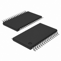
TDA8933BTW/N2,518 NXP Semiconductors, TDA8933BTW/N2,518 Datasheet - Page 12

TDA8933BTW/N2,518
Manufacturer Part Number
TDA8933BTW/N2,518
Description
IC AMP AUDIO 20.6W STER 32TSSOP
Manufacturer
NXP Semiconductors
Type
Class Dr
Datasheet
1.TDA8933BTWN2118.pdf
(42 pages)
Specifications of TDA8933BTW/N2,518
Output Type
1-Channel (Mono) or 2-Channel (Stereo)
Max Output Power X Channels @ Load
20.6W x 1 @ 16 Ohm; 10.3W x 2 @ 8 Ohm
Voltage - Supply
10 V ~ 36 V, ±5 V ~ 18 V
Features
Depop, Differential Inputs, Mute, Short-Circuit and Thermal Protection
Mounting Type
Surface Mount
Package / Case
32-TSSOP Exposed Pad, 32-eTSSOP, 32-HTSSOP
Lead Free Status / RoHS Status
Lead free / RoHS Compliant
Other names
935285222518
TDA8933BTW/N2-T
TDA8933BTW/N2-T
TDA8933BTW/N2-T
TDA8933BTW/N2-T
NXP Semiconductors
9. Internal circuitry
TDA8933B_1
Preliminary data sheet
8.7 Output voltage buffers
When pin POWERUP is set HIGH the half-supply output voltage buffers are switched on
in asymmetrical configuration. The start-up will then be pop-free because the device
starts switching when the capacitor on pin HVPREF and the SE capacitors are completely
charged.
Output voltage buffer pins:
Table 7.
Pin
1
16
17
32
2
3
12
14
15
•
•
•
Pins HVP1 and HVP2: The time required for charging the SE capacitor depends on its
value. The half-supply voltage output is disabled when the TDA8933B is used in a
symmetrical supply application.
Pin HVPREF: This output voltage reference buffer charges the capacitor on pin
HVPREF.
Pin INREF: This output voltage reference buffer charges the input reference capacitor
on pin INREF, which applies the bias voltage for the inputs.
Internal circuitry
Symbol
V
IN1P
IN1N
INREF
IN2N
IN2P
SSD(HW)
Rev. 01 — 23 October 2008
Equivalent circuit
2, 15
3, 14
12
17, 32
1, 16,
2 k
2 k
V
V
20 %
20 %
DDA
SSA
48 k
48 k
20 %
20 %
Class D audio amplifier
001aad784
TDA8933B
V
V
DDA
SSA
© NXP B.V. 2008. All rights reserved.
V/I
V/I
001aad785
HVPREF
12 of 42


