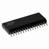
TDA8932BT/N2,112 NXP Semiconductors, TDA8932BT/N2,112 Datasheet - Page 11

TDA8932BT/N2,112
Manufacturer Part Number
TDA8932BT/N2,112
Description
IC AMP AUDIO 55W STER D 32SOIC
Manufacturer
NXP Semiconductors
Type
Class Dr
Datasheet
1.TDA8932BTWN2118.pdf
(48 pages)
Specifications of TDA8932BT/N2,112
Output Type
1-Channel (Mono) or 2-Channel (Stereo)
Package / Case
32-SOIC (7.5mm Width)
Max Output Power X Channels @ Load
55W x 1 @ 8 Ohm; 26.5W x 2 @ 4 Ohm
Voltage - Supply
10 V ~ 36 V, ±5 V ~ 18 V
Features
Depop, Differential Inputs, Mute, Short-Circuit and Thermal Protection
Mounting Type
Surface Mount
Product
Class-D
Output Power
55 W
Available Set Gain
36 dB
Common Mode Rejection Ratio (min)
75 dB
Thd Plus Noise
0.007 %
Operating Supply Voltage
22 V
Supply Current
145 mA
Maximum Power Dissipation
5000 mW
Maximum Operating Temperature
+ 85 C
Mounting Style
SMD/SMT
Audio Load Resistance
8 Ohms
Dual Supply Voltage
+/- 11 V
Input Signal Type
Differential
Minimum Operating Temperature
- 40 C
Output Signal Type
Differential, Single
Supply Type
Single or Dual
Supply Voltage (max)
36 V
Supply Voltage (min)
10 V
Lead Free Status / RoHS Status
Lead free / RoHS Compliant
Other names
935283477112
TDA8932BT
TDA8932BT
TDA8932BT
TDA8932BT
NXP Semiconductors
TDA8932B_4
Product data sheet
8.5 Diagnostic input and output
8.6 Differential inputs
8.7 Output voltage buffers
Whenever a protection other than TF is triggered, pin DIAG is forced LOW level (see
Table
approximately 2.4 V. This internal reference supply can deliver approximately 50 A.
Pin DIAG refers to pin CGND. The diagnostic output signal during different short
conditions is illustrated in
device into Fault mode.
For a high common-mode rejection ratio and a maximum of flexibility in the application,
the audio inputs are fully differential. By connecting the inputs anti-parallel, the phase of
one of the two channels can be inverted, so that the amplifier can operate as a mono BTL
amplifier. The input configuration for a mono BTL application is illustrated in
In SE configuration it is also recommended to connect the two differential inputs in
anti-phase. This has advantages for the current handling of the power supply at low signal
frequencies and minimizes supply pumping (see also
When pin POWERUP is set HIGH, the half supply output voltage buffers are switched on
in asymmetrical supply configuration. The start-up will be pop free since the device starts
switching when the capacitor on pin HVPREF and the SE capacitors are completely
charged.
Output voltage buffers:
Fig 6.
Fig 7.
6). An internal reference supply will pull-up the open-drain DIAG output to
Diagnostic output for different short-circuit conditions
Input configuration for mono BTL application
2.4 V
audio
0 V
input
V
o
Rev. 04 — 18 December 2008
Figure
50 ms
shorted load
IN1P
IN1N
IN2P
IN2N
6. Using pin DIAG as input, a voltage < 0.8 V will put the
50 ms
amplifier
restart
2.4 V
0 V
V
o
Section
OUT1
OUT2
14.8).
no restart
supply line
Class-D audio amplifier
short to
001aad760
001aad759
TDA8932B
© NXP B.V. 2008. All rights reserved.
Figure
11 of 48
7.


