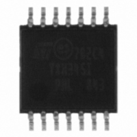
TSH345IPT STMicroelectronics, TSH345IPT Datasheet

TSH345IPT
Specifications of TSH345IPT
Available stocks
Related parts for TSH345IPT
TSH345IPT Summary of contents
Page 1
Features ■ Selectable 6th order filtering of 36 MHz, 18 MHz and 9 MHz ■ single-supply operation ■ Internal input DC level shifter ■ No input capacitor required ■ 3 matched 6 dB amplifiers ■ ...
Page 2
Absolute maximum ratings and operating conditions 1 Absolute maximum ratings and operating conditions Table 1. Absolute maximum ratings Symbol (1) V Supply voltage CC V Input voltage range in T Operating free air temperature range oper T Storage temperature stg ...
Page 3
TSH345 2 Electrical characteristics Table 3. Electrical characteristics at V (unless otherwise specified) Symbol DC performance Output DC shift -40° C < T Input bias current amb -40° C < T Input resistance, ...
Page 4
Electrical characteristics Table 3. Electrical characteristics at V (unless otherwise specified) (continued) Symbol Bandwidth F2 selected, small signal, V Standard -3 dB bandwidth definition -1 dB bandwidth with progressive Attenuation scanning F2 selected MHz, small signal, V ICM ...
Page 5
TSH345 Table 4. Filter and standby settings, V (1) Fs1 Fs0 Fs1 and Fs0 pins must never be left floating. Table 5. Mux settings, V (1) Mux The MUX pin must never ...
Page 6
Electrical characteristics Figure 1. Filtering 10 0 -10 -20 -30 Vcc=5V -40 small signal Ω Load=150 -50 1M 10M Frequency (Hz) Figure 3. Distortion 1 MHz (HD) 0 Vcc=5V -10 F=1MHz -20 HD filter Ω Load=150 -30 -40 -50 HD2 ...
Page 7
TSH345 Figure 7. Distortion 1 MHz (SD filter) 0 Vcc=5V -10 F=1MHz SD filter -20 Ω Load=150 -30 -40 -50 HD2 -60 -70 -80 HD3 -90 -100 0.0 0.5 1.0 1.5 2.0 Output Amplitude (Vp-p) Figure 9. Gain vs. input ...
Page 8
Electrical characteristics Figure 13. Current consumption vs. supply Vcc=5V no Load 0.0 0.5 1.0 1.5 2.0 2.5 Vcc (V) Figure 15. Filtering vs. temperature 40 Vcc=5V Ω Load=150 ...
Page 9
TSH345 Figure 19. Standby current vs. temperature 180 Vcc=5V no Load 170 160 150 140 130 120 -40 - Temperature (°C) Figure 21. Isource vs. temperature 120 110 100 Vcc=5V 50 -40 -20 0 ...
Page 10
Electrical characteristics Figure 25. Gain vs. temperature 2.20 2.15 2.10 2.05 2.00 1.95 1.90 Vcc=5V 1.85 Ω Load=150 1.80 -40 - Temperature (°C) 10/ TSH345 ...
Page 11
TSH345 2.1 Power supply considerations: improving the power supply noise rejection Correct power supply bypassing is very important to optimize performance in low- and high- frequency ranges. Bypass capacitors should be placed as close as possible to the IC pin ...
Page 12
Electrical characteristics Figure 27. Circuit for noise rejection improvement measurement +5 V Figure 28 shows how the power supply noise rejection evolves according to the frequency and depending on how carefully power supply decoupling is achieved. Figure 28. Power supply ...
Page 13
TSH345 Using the TSH345 to drive YC, CVBS, YUV, YPbPr and RGB video components 3 Using the TSH345 to drive YC, CVBS, YUV, YPbPr and RGB video components Figure 29. Implementation of the video driver on output video DACs Reconstruction ...
Page 14
Using the TSH345 to drive YC, CVBS, YUV, YPbPr and RGB video components Figure 30. Synchronization details (example for a black picture (2t) HD 300 mV 590 ns ( c.t ip 160 ...
Page 15
TSH345 Using the TSH345 to drive YC, CVBS, YUV, YPbPr and RGB video components Figure 32. Standard video signal 300 mV DAC’s offset GND (DAC’s offset on STi7200 = 28 mV) Video contents MHz 1.3 Vp-p (+/- ...
Page 16
Using the TSH345 to drive YC, CVBS, YUV, YPbPr and RGB video components Figure 33. Flexibility of the TSH345 for SD and HD signals HD/PV/SD Y,G DAC Pb,B,C DAC Pr,R,C DAC HD/PV/SD Y,G DAC Pb,B,C DAC Pr,R,C DAC The TSH345 ...
Page 17
TSH345 Using the TSH345 to drive YC, CVBS, YUV, YPbPr and RGB video components 3.1 Output capacitor The output can be either DC-coupled or AC-coupled. The output can be directly connected to the line via a 75-Ω resistor (see any ...
Page 18
Package information 4 Package information In order to meet environmental requirements, ST offers these devices in different grades of ® ECOPACK packages, depending on their level of environmental compliance. ECOPACK specifications, grade definitions and product status are available at: www.st.com. ...
Page 19
TSH345 4.1 SO-14 package information Figure 36. SO-14 package mechanical drawing Table 6. SO-14 package mechanical data Ref ddd Note: D and F dimensions do not include mold ...
Page 20
Package information 4.2 TSSOP14 package information Figure 37. TSSOP14 package mechanical drawing Table 7. TSSOP14 package mechanical data Ref aaa 20/23 Dimensions Millimeters Min. Typ. Max. 1.20 0.05 ...
Page 21
... TSH345 5 Ordering information Table 8. Order codes Part number TSH345ID TSH345IDT TSH345IPT Temperature Package range SO-14 -40°C to +85°C TSSOP14 Ordering information Packing Marking Tube TSH345I Tape & reel TSH345I Tape & reel TSH345I 21/23 ...
Page 22
Revision history 6 Revision history Table 9. Document revision history Date 29-May-2007 18-Dec-2008 22/23 Revision 1 Initial release. Added curves in Chapter 2: Electrical 2 Added all test limits in Changes characteristics. Chapter Table 3. TSH345 ...
Page 23
... TSH345 Information in this document is provided solely in connection with ST products. STMicroelectronics NV and its subsidiaries (“ST”) reserve the right to make changes, corrections, modifications or improvements, to this document, and the products and services described herein at any time, without notice. All ST products are sold pursuant to ST’s terms and conditions of sale. ...


