ISL4089IBZ-T7 Intersil, ISL4089IBZ-T7 Datasheet
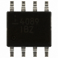
IC VIDEO AMP RESTORED 250MHZ SO8

ISL4089IBZ-T7

Manufacturer Part Number
ISL4089IBZ-T7
Description
IC VIDEO AMP RESTORED 250MHZ SO8
Manufacturer
Intersil
Datasheet

Specifications of ISL4089IBZ-T7

Applications
General Purpose
Number Of Circuits
1
-3db Bandwidth
300MHz
Slew Rate
300 V/µs
Current - Supply
20mA
Current - Output / Channel
100mA
Mounting Type
Surface Mount
Package / Case
8-SOIC (0.154", 3.90mm Width)
Lead Free Status / RoHS Status
Lead free / RoHS Compliant
Other names
ISL4089IBZ-T7TR
DC-Restored Video Amplifier
The ISL4089 is complete DC-restored monolithic video
amplifier sub-system. It contains a high performance video
amplifier and a nulling, sample-and-hold amplifier designed
to establish a programmable DC output level.
When the HOLD logic input “0” is applied the DC restore
function is active. The sample-and-hold amplifier loop is
closed and used to null the DC offset of the video amplifier.
This can occur during sync, or, at any time that a black level
is expected. When the HOLD input “1” is applied, the
correcting voltage is stored on the video amplifier’s input
coupling capacitor. This condition must be true during active
video. The restored DC voltage level can be adjusted using
an external reference voltage applied to the V
The device operates from a single +5V supply and is ideal
for +5V only systems when used with a sync separator, such
as the EL1883.
The ISL4089 is intended to directly replace the EL4089 only
in certain applications. This direct replacement requires that
the single positive supply is no higher than +5.5V and that no
part of the clamped output goes below ground. The NC on
pin 6 is not internally connected, so it can be connected to
the -5V pin in existing EL4089 applications.
The ISL4089 is specified for operation over -40°C to +85°C
temperature range.
Pinout
IN-
IN-
IN+
IN+
V
V
HOLD
HOLD
REF
REF
+
+
+
(8 Ld SOIC)
TOP VIEW
ISL4089
®
+
+
+
-
-
-
1
Data Sheet
REF
V+
V+
V
V
N/C
N/C
GND
GND
OUT
OUT
pin.
1-888-INTERSIL or 1-888-468-3774
CAUTION: These devices are sensitive to electrostatic discharge; follow proper IC Handling Procedures.
Features
• Complete video level DC-restoration system
• 0.03% differential gain and 0.05° differential phase
• 300MHz -3dB small signal bandwidth at A
• 150MHz -3dB small signal bandwidth at A
• 300V/µs Slew Rate
• 0.1dB flatness to 80MHz
• +5V single supply operation
• TTL/CMOS compatible hold signal
• Pb-free plus anneal available (RoHS compliant)
Applications
• Input amplifier in video equipment
• DC-restoration amplifier in video mixers
Related Documents
• AN1261: ISL4089EVAL1 User’s Guide
• AN1089: EL4089 and EL4390 DC-Restored Video
Ordering Information
NOTE: Intersil Pb-free plus anneal products employ special Pb-free
material sets; molding compounds/die attach materials and 100%
matte tin plate termination finish, which are RoHS compliant and
compatible with both SnPb and Pb-free soldering operations. Intersil
Pb-free products are MSL classified at Pb-free peak reflow
temperatures that meet or exceed the Pb-free requirements of
IPC/JEDEC J STD-020.
ISL4089IBZ
(See Note)
ISL4089IBZ-T7
(See Note)
PART NUMBER
accuracy
Amplifier
All other trademarks mentioned are the property of their respective owners.
June 28, 2006
|
Intersil (and design) is a registered trademark of Intersil Americas Inc.
4089IBZ
4089IBZ
Copyright © Intersil Americas Inc. 2006. All Rights Reserved.
MARKING
PART
TAPE &
REEL
7”
-
8 Ld SO
(Pb-free)
8 Ld SO
(Pb-free)
PACKAGE
ISL4089
V
V
= 1
= 2
FN6192.1
MDP0027
MDP0027
DWG. #
PKG.

Related parts for ISL4089IBZ-T7

ISL4089IBZ-T7 Summary of contents

Page 1

... AN1089: EL4089 and EL4390 DC-Restored Video Amplifier Ordering Information PART NUMBER ISL4089IBZ (See Note) ISL4089IBZ-T7 (See Note NOTE: Intersil Pb-free plus anneal products employ special Pb-free material sets; molding compounds/die attach materials and 100% matte tin plate termination finish, which are RoHS compliant and compatible with both SnPb and Pb-free soldering operations ...

Page 2

Absolute Maximum Ratings (T A Voltage between V+ and GND . . . . . . . . . . . . . . . . . . . . . . . . . . 5.5V Voltage between IN+, ...

Page 3

AC Electrical Specifications V PARAMETER DESCRIPTION 0.1dB BW 0.1dB Gain Flatness; Unity Gain 0.1dB Gain Flatness Differential Gain Error dP Differential Phase Error RESTORE SECTION T Time to Enable Hold; 50 Time to Disable ...

Page 4

Typical Performance Curves 0 475 150 L 0 -0.1 -0 OUT P-P -0.3 -0.4 -0.5 -0.6 -0.7 -0.8 1M 10M FREQUENCY (Hz) FIGURE 5. ...

Page 5

Typical Performance Curves JEDEC JESD51-7 HIGH EFFECTIVE THERMAL CONDUCTIVITY TEST BOARD 1 909mW 0.8 0.6 0.4 0 AMBIENT TEMPERATURE (°C) FIGURE 10. PACKAGE POWER DISSIPATION vs AMBIENT TEMPERATURE ISL4089 EQUIVALENT (8 LD SOIC) PIN ...

Page 6

AC Test Circuits 118Ω 86.6Ω 50Ω 1. HOLD INPUT = 1 FIGURE 12A. VIDEO AMPLIFIER AC TEST CIRCUIT FOR 50Ω ...

Page 7

R G 475Ω V IN- VIDEO INPUT CX1 V IN+ RX1 75Ω V REF - V Ref 0V to +4.5V FIGURE 13. BASIC +5V APPLICATION CIRCUIT Using the Reference Voltage Input (V Implementing DC-restore and amplifying composite video using a ...

Page 8

R4 R4 475 ohms 475 ohms C4 C4 0.01uF 0.01uF VIDEO VIDEO INPUT INPUT ohms 75 ohms Composite Sync Composite Sync Out Out C5 C5 0.1uF 0.1uF Vertical Sync Vertical Sync Out Out FIGURE 14. APPLICATION CIRCUIT ...

Page 9

... Accordingly, the reader is cautioned to verify that data sheets are current before placing orders. Information furnished by Intersil is believed to be accurate and reliable. However, no responsibility is assumed by Intersil or its subsidiaries for its use; nor for any infringements of patents or other rights of third parties which may result from its use ...

Related keywords