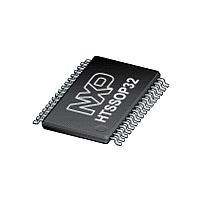
TDA8933B NXP Semiconductors, TDA8933B Datasheet - Page 6

TDA8933B
Manufacturer Part Number
TDA8933B
Description
The TDA8933B is a high-efficiency class D amplifier with low power dissipation
Manufacturer
NXP Semiconductors
Datasheet
1.TDA8933B.pdf
(42 pages)
Available stocks
Company
Part Number
Manufacturer
Quantity
Price
Part Number:
TDA8933BTW
Manufacturer:
NXP/恩智浦
Quantity:
20 000
Company:
Part Number:
TDA8933BTW/N2@118
Manufacturer:
NXP
Quantity:
2 250
NXP Semiconductors
TDA8933B_1
Preliminary data sheet
8.2 Mode selection and interfacing
The TDA8933B can be switched to one of four operating modes using pins POWERUP
and ENGAGE:
Both pins POWERUP and ENGAGE refer to pin CGND.
Table 4
ENGAGE pins.
Table 4.
[1]
If the transition between Mute mode and Operating mode is controlled via a time constant,
the start-up will be pop-free since the DC output offset voltage is applied gradually to the
output. The bias current setting of the V/I-converters is related to the voltage on pin
ENGAGE.
The time constant required to apply the DC output offset voltage gradually between Mute
mode and Operating mode can be generated by applying a capacitor on pin ENGAGE.
The value of the capacitor on pin ENGAGE should be 470 nF.
Mode
Sleep
Mute
Operating
Fault
•
•
•
•
•
•
Sleep mode: with low supply current.
Mute mode: the amplifiers are switching to idle (50 % duty cycle), but the audio signal
at the output is suppressed by disabling the V
on pins HVP1 and HVP2 have been charged to half the supply voltage (asymmetrical
supply only)
Operating mode: the amplifiers are fully operational with an output signal
Fault mode
When there are symmetrical supply conditions, the voltage applied to pins POWERUP and ENGAGE must
never exceed the supply voltage (V
Mute mode: the bias current setting of the V/I-converters is zero (V/I-converters
disabled).
Operating mode: the bias current is at maximum.
shows the different modes as a function of the voltages on the POWERUP and
Mode selection for the TDA8933B
Rev. 01 — 23 October 2008
Pin
POWERUP
< 0.8 V
2 V to 6 V
2 V to 6 V
2 V to 6 V
DDA
[1]
, V
DDP1
or V
DDP2
ENGAGE
< 0.8 V
< 0.8 V
2.4 V to 6 V
undefined
).
l
-converter input stages. The capacitors
[1]
Class D audio amplifier
TDA8933B
DIAG
undefined
> 2 V
> 2 V
< 0.8 V
© NXP B.V. 2008. All rights reserved.
6 of 42


