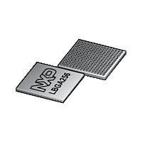
LPC1850FET256 NXP Semiconductors, LPC1850FET256 Datasheet - Page 21

LPC1850FET256
Manufacturer Part Number
LPC1850FET256
Description
The LPC1850FET256 is a high-performance, cost-effective Cortex-M3 microcontroller featuring 200 kB of SRAM, and advanced peripherals including Ethernet, High Speed USB 2
Manufacturer
NXP Semiconductors
Datasheet
1.LPC1810FBD144.pdf
(157 pages)
Available stocks
Company
Part Number
Manufacturer
Quantity
Price
Company:
Part Number:
LPC1850FET256
Manufacturer:
NXP
Quantity:
1 000
Part Number:
LPC1850FET256
Manufacturer:
NXP/恩智浦
Quantity:
20 000
Company:
Part Number:
LPC1850FET256,551
Manufacturer:
NXP Semiconductors
Quantity:
10 000
Part Number:
LPC1850FET256,551
Manufacturer:
NXP/恩智浦
Quantity:
20 000
NXP Semiconductors
Table 3.
LCD, Ethernet, USB0, and USB1 functions are not available on all parts. See
LPC1850_30_20_10
Preliminary data sheet
Symbol
P3_4
P3_5
P3_6
Pin description
A15
C12
B13
x
x
x
…continued
B8
B7
C7
171 119
174 122 85
173 121 84
All information provided in this document is subject to legal disclaimers.
Rev. 3.1 — 15 December 2011
82
[3]
[3]
[3]
I; PU I/O GPIO1[14] — General purpose digital input/output
I; PU I/O GPIO1[15] — General purpose digital input/output
I; PU I/O GPIO0[6] — General purpose digital input/output pin.
-
-
I/O SPIFI_SIO3 — I/O lane 3 for SPIFI.
O
I/O I2S0_TX_WS — Transmit Word Select. It is driven by
I/O I2S1_RX_SDA — I
O
-
-
I/O SPIFI_SIO2 — I/O lane 2 for SPIFI.
I
I/O I2S0_TX_SDA — I
I/O I2S1_RX_WS — Receive Word Select. It is driven by
O
-
I/O SSP0_SSEL — Slave Select for SSP0.
I/O SPIFI_MISO — Input 1 in SPIFI quad mode; SPIFI
-
I/O SSP0_MISO — Master In Slave Out for SSP0.
-
-
Description
pin.
R — Function reserved.
R — Function reserved.
U1_TXD — Transmitter output for UART1.
the master and received by the slave. Corresponds
to the signal WS in the I
the transmitter and read by the receiver. Corresponds
to the signal SD in the I
LCD_VD13 — LCD data.
pin.
R — Function reserved.
R — Function reserved.
U1_RXD — Receiver input for UART1.
transmitter and read by the receiver. Corresponds to
the signal SD in the I
the master and received by the slave. Corresponds
to the signal WS in the I
LCD_VD12 — LCD data.
R — Function reserved.
output IO1.
R — Function reserved.
R — Function reserved.
R — Function reserved.
Table
32-bit ARM Cortex-M3 microcontroller
LPC1850/30/20/10
2.
2
2
S transmit data. It is driven by the
S1 receive data. It is driven by
2
S-bus specification.
2
2
2
S-bus specification.
S-bus specification.
S-bus specification.
© NXP B.V. 2011. All rights reserved.
21 of 157


