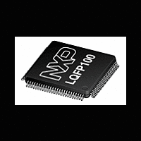
LPC2387FBD100 NXP Semiconductors, LPC2387FBD100 Datasheet - Page 5

LPC2387FBD100
Manufacturer Part Number
LPC2387FBD100
Description
The LPC2387 is an ARM7 microcontroller for embedded applications featuring a high level of integration and low power consumption at frequencies of 72 MHz
Manufacturer
NXP Semiconductors
Datasheet
1.LPC2387FBD100.pdf
(66 pages)
Available stocks
Company
Part Number
Manufacturer
Quantity
Price
Company:
Part Number:
LPC2387FBD100
Manufacturer:
NXP
Quantity:
3 000
Part Number:
LPC2387FBD100
Manufacturer:
NXP/恩智浦
Quantity:
20 000
Company:
Part Number:
LPC2387FBD100,551
Manufacturer:
NXP Semiconductors
Quantity:
10 000
NXP Semiconductors
6. Pinning information
Table 3.
LPC2387
Product data sheet
Symbol
P0[0] to P0[31]
P0[0]/RD1/TXD3/
SDA1
P0[1]/TD1/RXD3/
SCL1
P0[2]/TXD0
P0[3]/RXD0
P0[4]/I2SRX_CLK/
RD2/CAP2[0]
Fig 2.
LPC2387 pinning LQFP100 package
Pin description
6.1 Pinning
6.2 Pin description
Pin
46
47
98
99
81
[1]
[1]
[1]
[1]
[1]
Type
I/O
I/O
I
O
I/O
I/O
O
I
I/O
I/O
O
I/O
I
I/O
I/O
I
I
All information provided in this document is subject to legal disclaimers.
Description
Port 0: Port 0 is a 32-bit I/O port with individual direction controls for each bit.
The operation of port 0 pins depends upon the pin function selected via the pin
connect block. Pins 12, 13, 14, and 31 of this port are not available.
P0[0] — General purpose digital input/output pin.
RD1 — CAN1 receiver input.
TXD3 — Transmitter output for UART3.
SDA1 — I
P0[1] — General purpose digital input/output pin.
TD1 — CAN1 transmitter output.
RXD3 — Receiver input for UART3.
SCL1 — I
P0[2] — General purpose digital input/output pin.
TXD0 — Transmitter output for UART0.
P0[3] — General purpose digital input/output pin.
RXD0 — Receiver input for UART0.
P0[4] — General purpose digital input/output pin.
I2SRX_CLK — Receive Clock. It is driven by the master and received by the
slave. Corresponds to the signal SCK in the I
RD2 — CAN2 receiver input.
CAP2[0] — Capture input for Timer 2, channel 0.
25
1
Rev. 5 — 9 January 2012
LPC2387FBD100
2
2
C1 clock input/output (this is not an open-drain pin).
C1 data input/output (this is not an open-drain pin).
002aad329
75
51
2
S-bus specification.
Single-chip 16-bit/32-bit MCU
LPC2387
© NXP B.V. 2012. All rights reserved.
5 of 66


