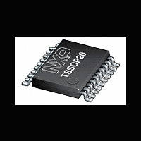
P89LPC924_925 NXP Semiconductors, P89LPC924_925 Datasheet - Page 7

P89LPC924_925
Manufacturer Part Number
P89LPC924_925
Description
The P89LPC924/925 are single-chip microcontrollers designed for applicationsdemanding high-integration, low cost solutions over a wide range of performancerequirements
Manufacturer
NXP Semiconductors
Datasheet
1.P89LPC924_925.pdf
(49 pages)
Philips Semiconductors
Table 3:
9397 750 14471
Product data
Symbol
P1.0 - P1.7
Pin description
Pin
12, 11, 10,
9, 8, 4, 3,
2
12
11
10
9
8
4
3
2
Type
I/O, I
I/O
O
I/O
I
I/O
I/O
I/O
I/O
I
I/O
I/O
I
I
I
I/O
I/O
…continued
[1]
Description
Port 1: Port 1 is an 8-bit I/O port with a user-configurable output type, except for three
pins as noted below. During reset Port 1 latches are configured in the input only mode
with the internal pull-up disabled. The operation of the configurable Port 1 pins as inputs
and outputs depends upon the port configuration selected. Each of the configurable
port pins are programmed independently. Refer to
and
used as outputs. P1.5 is input only.
All pins have Schmitt triggered inputs.
Port 1 also provides various special functions as described below:
P1.0 — Port 1 bit 0.
TXD — Transmitter output for the serial port.
P1.1 — Port 1 bit 1.
RXD — Receiver input for the serial port.
P1.2 — Port 1 bit 2 (open-drain when used as output).
T0 — Timer/counter 0 external count input or overflow output (open-drain when used as
output).
SCL — I
P1.3 — Port 1 bit 3 (open-drain when used as output).
INT0 — External interrupt 0 input.
SDA — I
P1.4 — Port 1 bit 4.
INT1 — External interrupt 1 input.
P1.5 — Port 1 bit 5 (input only).
RST — External Reset input (if selected via FLASH configuration). A LOW on this pin
resets the microcontroller, causing I/O ports and peripherals to take on their default
states, and the processor begins execution at address 0. When using an oscillator
frequency above 12 MHz, the reset input function of P1.5 must be enabled. An
external circuit is required to hold the device in reset at power-up until V
reached its specified level. When system power is removed V
minimum specified operating voltage. When using an oscillator frequency above
12 MHz, in some applications, an external brownout detect circuit may be
required to hold the device in reset when V
operating voltage.
P1.6 — Port 1 bit 6.
P1.7 — Port 1 bit 7.
Table 8 “DC electrical characteristics”
2
2
C serial clock input/output.
C serial data input/output.
Rev. 03 — 15 December 2004
8-bit microcontrollers with accelerated two-clock 80C51 core
for details. P1.2 - P1.3 are open drain when
DD
falls below the minimum specified
Section 8.13.1 “Port configurations”
P89LPC924/925
© Koninklijke Philips Electronics N.V. 2004. All rights reserved.
DD
will fall below the
DD
has
7 of 49


