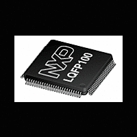
XA-H4 NXP Semiconductors, XA-H4 Datasheet - Page 20

XA-H4
Manufacturer Part Number
XA-H4
Description
The powerful 16-bit XA CPU core and rich feature set make the XA-H3 and XA-H4 devices ideal for high-performance real-time applications such as industrial control and networking
Manufacturer
NXP Semiconductors
Datasheet
1.XA-H4.pdf
(42 pages)
Philips Semiconductors
memory bank or peripheral can be programmed to accommodate
slow or fast devices.
Each memory bank and its associated RAS (chip select in DRAM
mode) output, can be programmed to access up to an 8 MB
mappable address space in either EDO or FPM DRAM modes (up
to a total of 32 MB of DRAM. WARNING: Future XA-H4 derivatives
may not support separate code and data spaces.)
Bus Interface Pins
For the following discussion, see Figure 3.
1999 Sep 24
WARNING: On the external bus, ALL XA-H4 reads are 16-bit Reads. If the CPU instruction only specifies 8-bits, then the CPU uses the appropriate
byte, and discards the extra byte. Thus “8-Bit Reads” and “16-Bit Reads” appear to be identical on the bus. On an 8-bit bus, this will appear
as two consecutive 8-bit reads even though the CPU instruction specified a byte read.
Some 8-bit I/O devices (especially FIFOs) cannot operate correctly with 2 bytes being read for a 1 Byte Read. The most common (and least
expensive) solution is to operate these 8-bit devices on a 16-bit bus, and access them in software on all odd byte (or all even byte) boundaries.
An added benefit of this technique is that byte Reads are faster than on an 8-bit bus, because only 1 word is fetched (a single Read) instead of
2 consecutive bytes.
Single-chip 16-bit microcontroller
DRAM Controller
SRAM Controller
Dynamic Bus Sizing
Progammable Bus Timing
Figure 3. Memory bus interface signal pins
Memory Interface
XA-H4
20
Each memory bank and associated chip select programmed for
“generic” (SRAM, Flash, ROM, peripheral chips, etc.) is capable of
supporting a 1 MB address space.
The Memory Interface can be programmed to support both Intel
style and 68000 bus style SRAMs and peripherals.
Chip Select Pins
There are six chip select pins (CS5 – CS0) mapped to six sets of bank
control registers. The following attributes are individually programmable
for each bank and associated chip select (or RAS, if DRAM): bank
on/off, address range, external device access time, detailed bus strobe
sequence, DRAM cycle or generic bus cycle, DRAM size if DRAM,
and bus width. Pin CS0 is always generic in order to service the boot
device, thus CS0 cannot be connected to DRAM.
CS5 or RAS5 (or P3.1, RTS1)
CS4 or RAS4 (or P3.0, RTClk1)
CS3 or RAS3
CS2 or RAS2
CS1 or RAS1
CS0
ClkOut
BHE or CASH
BLE or CASL
OE
WE
WAIT, SIZE16
D15–D0
A19–A0
(on DRAM cycle, A22 – A0
are Time-Multiplexed for RAS/CAS)
Preliminary specification
SU01274
XA-H4


